NVIDIA's 1.4 Billion Transistor GPU: GT200 Arrives as the GeForce GTX 280 & 260
by Anand Lal Shimpi & Derek Wilson on June 16, 2008 9:00 AM EST- Posted in
- GPUs
Building NVIDIA's GT200
Here's a Streaming Processor, NVIDIA calls it an SP:
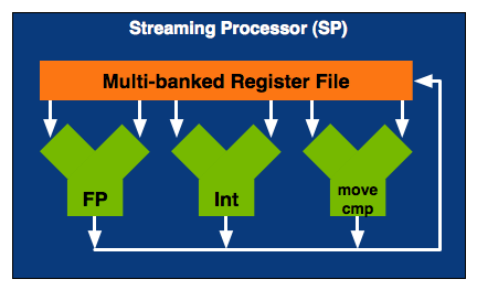
NVIDIA calls an individual SP a single processing core, which is actually true. It is a fully pipelined, single-issue, in-order microprocessor complete with two ALUs and a FPU. An SP doesn't have any cache, so it's not particularly great at anything other than cranking through tons of mathematical operations. Since an SP spends most of its time working on pixel or vertex data, the fact that it doesn't have a cache doesn't really matter. Aside from name similarities, one NVIDIA SP is a lot like a very simplified version of a SPE in the Cell microprocessor (or maybe the SPE is like a really simple version of one of NVIDIA's SMs, which we'll get to in a minute). While a single SPE in Cell has seven execution units, a single NVIDIA SP only has three.
By itself a SP is fairly useless, but NVIDIA builds GPUs and if you add up enough of these little monsters you can start to get something productive given that graphics rendering is a highly parallelizable task.
Here's a Streaming Multiprocessor, which NVIDIA abbreviates as SM:

A SM is an array of SPs, eight to be specific, along with two more processors called Special Function Units (SFUs). Each SFU has four FP multiply units which are used for transcendental operations (e.g. sin, cosin) and interpolation, the latter being used in some of the calculations for things like anisotropic texture filtering. Although NVIDIA isn't specific in saying so, we assume that each SFU is also a fully pipelined, single-issue, in-order microprocessor. There's a MT issue unit that dispatches instructions to all of the SPs and SFUs in the group.
In addition to the processor cores in a SM, there's a very small instruction cache, a read only data cache and a 16KB read/write shared memory. These cache sizes are kept purposefully small because unlike a conventional desktop microprocessor, the datasets we're trying to cache here are small. Each SP ends up working on an individual pixel and despite the move to 32-bit floating point values, there's only so much data associated with a single pixel. The 16KB memory is akin to Cell's local stores in that it's not a cache, but a software-managed data store so that latency is always predictable. With this many cores in a single SM, control and predictability and very important to making the whole thing work efficiently.
Take one more step back and you've got a Texture/Processor Cluster (TPC):
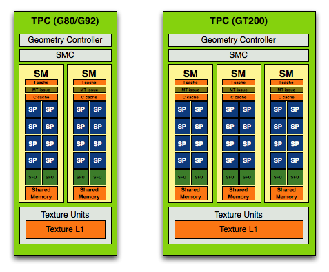
The G80/G92 TPC (left) vs. the GT200 TPC (right)
NVIDIA purposefully designed its GPU architecture to be modular, so a single TPC can be made up of any number of SMs. In the G80 architecture it was made up of two SMs but with the GT200 architecture it now has three SMs.
The components of the TPC however haven't changed; a TPC is made up of SMs, some control logic and a texture block. Remember that a SM is a total of 8 SPs and 2 SFUs, so that brings the total up to 24 SPs and 6 SFUs (must...not...type...STFU) per cluster in GT200 (up from 16 SPs and 4 SFUs in G80). The texture block includes texture addressing and filtering logic as well as a L1 texture cache.
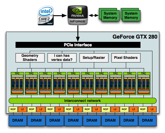
The modular theme continues with the Streaming Processor Array (SPA) that is composed of a number of TPCs:
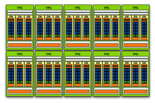
The GT200 SPA, that's 240 SPs in there if you want to count them
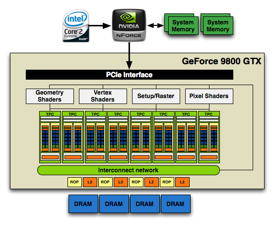
In G80 the SPA was made up of 8 TPCs, but with GT200 we've moved up to 10. Note that each TPC now has 3 SMs vs. 2, so the overall processing power of GT200 has increased by 87.5% over G80.
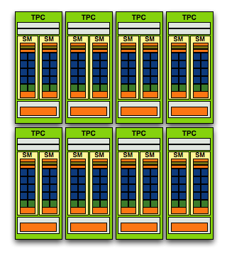
And here's G80/G92, only 128 SPs thanks to two SMs per TPC and 8 TPCs
At the front end of the GPU we've got schedulers and control logic to distribute workloads to the entire array of processing cores. At the other end we've got L2 texture caches and rasterization processors that handle final filtering and output of data to the frame buffer.
The culmination of all of this is that the new GT200 GPU, the heart of the GeForce GTX 280 and 260, features 240 SPs, 160KB of local memory, an even smaller amount of cache and is built on TSMC's 65nm process using 1.4 billion transistors.
1.4 Billion Transistors. It wants vertex data. Really bad.
754 Million Transistors
There are more transistors in this chip than there are people in China, and it's the largest, most compute-dense chip we've ever reviewed.


108 Comments
View All Comments
elchanan - Monday, June 30, 2008 - link
VERY eye-opening discussion on TMT. Thank you for it.I've been trying to understand how GPUs can be competitive for scientific applications which require lots of inter-process communication, and "local" memory, and this appears to be an elegant solution for both.
I can identify the weak points of it being hard to program for, as well as requiring many parallel threads to make it practical.
But are there other weak points?
Is there some memory-usage profile, or inter-process data bandwidth, where the trick doesn't work?
Perhaps some other algorithm characteristic which GPUs can't address well?
Think - Friday, June 20, 2008 - link
This card is a junk bond when taking into consideration cost/perfomance/power consumption.Reminds me of a 1976 Cadillac with a 7.7litre v8 with only 210 horsepower/3600 rpm.
It's a PIG.
Margalus - Tuesday, June 24, 2008 - link
this shows how many people don't run a dual monitor setup. I would snatch up one of these 260/280's over the gx2's anyday, gladly!!The performance may not be quite as good as an sli setup, but it will be much better than a single card which is what a lot of us are stuck with since you CANNOT run a dual monitor setup with sli!!!!!!!!!!!!!!!!!!!!!!!!!!!!!!!!!!!!!!!!!!!!!!!!!!!!!!!!
iamgud - Wednesday, June 18, 2008 - link
"I can has vertex data"LOL
These look fine, but need to be moved to 55nm. By the time I save up for one they will .
calyth - Tuesday, June 17, 2008 - link
Well what the heck are they doing with 1.4B transistors, which is becoming the largest die that TMSC has been producing so far?The larger the core, the more likely that an blemish would take out the core. As far as I know, didn't Phenom (4 cores on die) suffered low-yield problems?
gochichi - Tuesday, June 17, 2008 - link
You know, when you consider the price and you look at the benchmarks, you start looking for features and NVIDIA just doesn't have the features going on at all.COD4 -- Ran perfect at 1920x1200 with last gen stuff (the HD3870 and 8800GT(S))so now the benchmarks have to be for outrageous resolutions that a handful of monitors can handle (and those customers already bought SLI or XFIRE, or GTX2 etc.)
Crysis is a pig of a game, but it's not that great (it is a good technical preview though, I admit), and I don't think even these new cards really satisfy this system hog... so maybe this is a win, but I doubt too many people care... if you had an 8800GT or whatever, you're already played this game "well enough" on medium settings and are plenty tired of it. Though we'll surely fire it up in the future once our video cards "happen to be able to run it on high" very few people are going to go out of their way $500+ for this silly title.
In any case, then you look at ATI, and they have the HDMI audio, the DX 10.1 support and all they have to do at this point is A) Get a good price out the door, B) Make a good profit (make them cheap, which these NVIDIA are expensive to make, no doubt) and C) handily beat the 8800GTS and many of us are going to be sold.
These cards are what I would call a next gen preview. Some overheated prototypes of things to come. I doubt AMD will be as fast, and in fact I hope they aren't just as long as they keep the power consumption in check, the price, and the value (HDMI, DX10.1, etc).
Today's release reminded me that NVIDIA is the underdog, they are the company that released the FX series (desperate technology, like these are). ATI has been around well before 3DFX made 3d-accelerators. They were down for a bit, and we all said it was over for ATI but this desperate release from NVIDIA makes me think that ATI is going to be quite tought to beat.
Brazofuerte - Tuesday, June 17, 2008 - link
Can I go somewhere to find the exact settings used for these benchmarks? I appreciate the tech side of the write up but when it comes to determining whether I want one of these for my gaming machine (I ordered mine at midnight), I find HardOCP's numbers much more useful.woofermazing - Tuesday, June 17, 2008 - link
AMD/ATI isn't going to abandon the high end like your article implies. Their plan is to make a really good mid range chip, and ductape to cores together ala the X2's. Nvidia goes from the high-end down, ATI from the mid-end up. From the look of it, ATI might have the right idea, atleast this time around. I seriously doubt we'll see a two core version of this monster anytime soon.DerekWilson - Tuesday, June 17, 2008 - link
they are abandoning the high end single GPU ...we did state that they are planning on competing in the high end space with multiGPU cards, but that there are drawbacks to that.
we'll certainly have another article coming out sometime soon that looks a little more closely at AMD's strategy.
KeypoX - Tuesday, June 17, 2008 - link
i dont like it, not impressed either :(. Hopefully my 8800gt last for a while, far past this crap atleast