ASUS Striker II Extreme: Mucho Bang, Mucho Bucks
by Kris Boughton on April 11, 2008 7:00 AM EST- Posted in
- Motherboards
Complete BIOS Tuning Guide - "Extreme Tweaker" (Cont'd)
FSB - Memory Ratio - [Auto, 5:4, 3:2, Sync Mode] This field becomes available when FSB - Memory Clock Mode is set to Linked. The DRAM:FSB divider can then be manually adjusted using this setting.
For those unfamiliar with the concept, a memory divider defines the number of DRAM clocks for each tick of the FSB clock. Memory is said to be running synchronously with the system bus when it is operating at the same base frequency as the Front Side Bus (FSB). Differences in the perceived frequencies come from the manner in which memory and bus speeds are calculated. For example, if a system FSB is said to be operating at 1600MT/s (mega transfers per second) then the true frequency is only 400MHz, on account of the quad-pumped transfer protocol which allows for up to four separate data transmissions for each tick of the clock.
Memory running synchronously at 400MHz would also be operating at a base frequency of 400MHz, except that today's double data rate (DDR) memory is designed to accommodate up to two data transfers per cycle, resulting in a rated speed of DDR(x)-800. This explanation holds true, regardless of whether DDR, DDR2, or DDR3 memory is used. The ratio of these rated speeds is therefore 2:1 (1600MT/s to 800MT/s); however, because the established convention makes use of the actual base frequency (400MHz) the resulting ratio is actually calculated as 1:1 (400MHz to 400MHz). This matches well with our previous definition of synchronous memory operations.
A memory divider seeks to change the ratio of base memory clocks to system memory clocks so that it is possible to run system memory at frequencies higher than those dictated by system bus speed alone. For example, a memory divider of 6:5 (DRAM:FSB) means that for every five clocks of the FSB the installed memory bus undergoes six clock ticks. At 333MHz FSB, this is mathematically equivalent to 333MHz times 6 divided by 5 or 400MHz, which as we know would be DDR(x)-800. This is how processors based on a 333Mhz (1333MT/s) FSB are able to run memory at rated speeds of DDR(x)-800 without the need for any "traditional" overclocking.
One of the main differences between DDR2 and DDR3 memory standards is the frequency range the modules are designed to achieve. Although it is possible to buy DDR3-1066 memory, products offered at speeds such as these (and lower) are normally reserved for DDR2 while most DDR3 modules are sold as being capable of DDR3-1333 speeds or higher (frequencies well above the range of typical DDR2 modules). Because of this, synchronous memory operation takes on a new meaning when referring to DDR3 memory; instead of 1:1 memory operation, with DDR3 memory we are now implying 2:1. That is, the memory will run at exactly twice the base frequency of the FSB.
For example, a 333MHz FSB CPU (1333MT/s) times 2 divided by 1 yields 667MHz. Now convert this to the standard DDR naming convention (multiply by 2) and we have DDR(x)-1333. In this case, we are dealing with DDR3 memory so we call it DDR3-1333. If we were to select Sync Mode (read as 2:1) at 333MHz FSB our memory would be set to 1333 (really just 667MHz).
Coincidently, selecting Sync Mode results in the highest level of performance for whatever the current FSB happens to be. "Unlinking" the memory speed from the FSB and choosing a lower or higher target memory frequency will always result in a loss of memory read performance - no matter the case. We can't stress this enough: if you want more memory performance keep these two clocking domains closely coupled by setting FSB - Memory Clock Mode to "Linked". Make sure this option is set to Sync Mode, and then push up the FSB using the FSB (QDR), MHz field. Keep in mind you may need to reduce the CPU multiplier or increase the core voltage as you begin to overclock your processor.
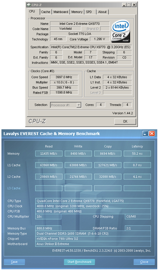
Our Intel QX9770 at 400MHz FSB with the memory running "linked 'n synced" at DDR3-1600 performs beautifully, pulling down well over 11GB/s in memory read performance.
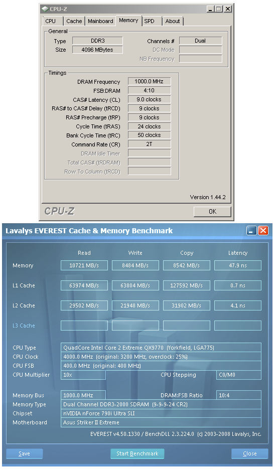
Our attempt at gaining more performance backfires when we unlink the memory and go to DDR3-2000. We actually lose more than 500MB/s in memory read performance at a higher memory speed.
The first option, Auto, represents whatever ratio is needed to set the memory for DDR3-1333 operation if a 333MHz (1333MT/s) CPU or 400MHz (1600MT/s) CPU is installed or DDR3-1066 operation if a 266MHz (1066MT/s) CPU is installed. This means Sync Mode (2:1) is set for every installed CPU with the exception of the QX9770, which actually defaults to a 6:5 ratio. In this particular case, a loss of performance will ensue unless the user (mandating DDR3-1600 operation) sets Sync Mode, and not Auto. Do yourself a favor and buy memory rated no lower than DDR3-1600 if you plan on ever moving up to the QX9700 or overclocking your CPU with this board to 400MHz FSB and higher. Do not let the relatively low prices of "value" DDR3 rated at 1333 or lower tempt you into a purchase unless you know it will overclock well.
FSB (QDR), MHz This is the target FSB, displayed in quad-data rate (QDR) format. Just realize that you should quadruple (x4) the actual base frequency desired when entering this value. The actual FSB (actual FSB MHz - quad-pumped) is shown directly below this setting and should always match what you enter here.
MEM (DDR), MHz This option that allows the user to type in a target memory speed and will only be available for direct edit when choosing "Unlinked" under FSB - Memory Clock Mode. Otherwise, this is automatically filled in based on the current FSB (QDR), MHz and FSB - Memory Ratio.
You may notice a slight offset from this target frequency, reflected in Actual MEM (DDR), MHz, when clocking your memory using the "Unlinked" mode of operation. This is normal and is due to the limited number of actual non-standard dividers implemented by the chipset used to give the illusion of fully dissociated clocking domains for the system and memory busses.
LDT Frequency - [1x ~ 5x] LDT (Lightning Data Transport) technology, licensed by NVIDIA from AMD, provides the interface pathway used to connected the 790i SPP with the 570 MCP. This setting should really be named "LDT Multiplier" as the final SPP-to-MCP link speed is set by multiplying this value by SPP<->MCP Ref Clock, MHz.
PCIE Bus, Slot 1 & 2 MHz PCIe x16 Slots 1 and 2 (blue in color) are PCI Express 2.0 compatible slots and should be used for the primary graphics controllers when running SLI. This field controls the base link speed between devices installed in these slots and the 790i SPP. Changing this from the default 100MHz value would always hang our Vista x64 system during OS load when the video drivers were first initialized.
PCIE Bus, Slot 3, MHz PCIe x16 Slot 3 (white in color) is the single PCI Express 1.x compatible slot. This field controls the base link speed between the device installed in this slot and the 570 MCP. Overclocking this interface will have absolutely no effect on graphics performance unless a third graphics controller is installed in this slot and is being used for 3-way SLI.
SPP<->MCP Ref Clock, MHz This field sets the base frequency of the SPP-to-MCP LDT interface link. In theory, a higher link speed, coupled with the highest possible multiplier (LDT Frequency) - resulting in the maximum stable link speed - should result in better system performance. However, unless you are running a 3-way SLI configuration and can show real gains by overclocking this interface, this is best left set to Auto. Unusually high link speeds have the potential to cause problems such as disk corruption, loss of RAID arrays, or memory access errors for DMA-connected devices.
SLI-Ready Memory - [Disabled, CPUOC 0% ~ CPUOC 5%, CPUOC MAX] Leave this setting on Disabled when manually overclocking memory. Selecting any other option will set DDR3-2000 memory operation - we were unable to measure any difference between any of the "CPU OC x%" options. Make sure you either manually adjust your memory timings or leave them on "Auto" if you plan on overclocking your memory this way.


23 Comments
View All Comments
seamusmc - Friday, April 11, 2008 - link
For folks considering this board, I strongly recommend visiting xstremesystems.org's forums.Several people are experiencing data/OS corruption when performing any FSB overclocking. (Brings back memories of the early days of the 680i.)
nomagic - Friday, April 11, 2008 - link
LGA775 Core2 Duo/Extreme/Quad, Pentium EE, Pentium D, Pentium including next-generation 45nm CPU supportWhich would include Nehalem, I suppose? Should I also assume that a BIOS update would be required for Nahalem support? Is it possible that a custom board like this might have trouble supporting Nehalem when the times comes?
TemjinGold - Friday, April 11, 2008 - link
No. NOTHING out right now can support Nehalem as that's a completely different socket (different pin count too).