Intel's Atom Architecture: The Journey Begins
by Anand Lal Shimpi on April 2, 2008 12:05 AM EST- Posted in
- CPUs
A Prelude to Success
This all started back in 2004, in Austin, Texas. Despite the location, I am talking about Intel and not AMD. In 2004, Intel's Austin Design Center was hard at work on another member of the Pentium 4 processor family - codenamed Tejas.
Tejas was scheduled to arrive after Prescott and continue the NetBurst lineage, but as history would have it, Tejas never saw the light of day. The project was canceled and Intel's corporate attention was instead shifted to taking the Pentium M architecture and improving it to be desktop-worthy.
The Tejas team was, as you'd expect, not particularly pleased with their project being canceled. But, as seems to be the case with Intel's best engineers and canceled projects, they channeled their disappointment into passion and excitement for their next design.
I should stop the story here and point out the striking similarity to another Intel success story, that of the original Centrino. Banias was the first Centrino processor, later named the Pentium M. The team that worked on Banias was the same team that worked on Timna, yet another project cancelled very late in the process. After Timna was cancelled the team, working out of Intel's Israel Design Center, went into a brief collective depression for about a month before receiving instructions to work on Banias. Instead of producing something mediocre, the team felt a need to prove something to those who cancelled their beloved Timna project. The result was Banias, which became the Pentium M, led to the Core Duo and eventually gave us the Core 2 family of processors that we love so dearly today.
Back to Austin. We've got a very small team of people who were hard at work on Tejas and now without anything to do. The same sense of proving their worth brew and in 2004 the team received new orders.
The task was to develop a low power, IA (Intel Architecture, read: x86) core for use in a many-core CPU design. Since this core would be used in a many-core CPU, it would have to be very, very low power (you can't have 10s of cores each consuming 100W).
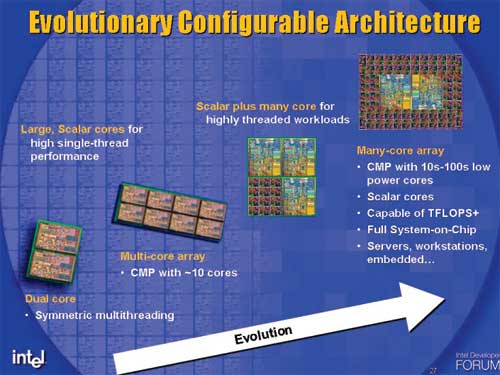
Many-core CPU designs are in Intel's future, Atom has its roots in the many-core initiative
I asked the design team in Austin if this was a dirty joke played on them by upper management - going from a very power hungry design like Tejas to something that would consume a couple of watts. Apparently during Tejas' design, a smaller team in Austin was doing some pathfinding work, looking at very low power simple cores. Since they spent about a year doing this pathfinding work, the transition from Tejas to something very low power was natural despite what it may seem from the outside.
Many of the architects that would work on this new, low power core actually came from other microprocessor companies. Belli Kuttanna, the chief architect on the core, worked for Sun on SPARC processors as well as Motorola designing elements of PowerPC cores. Belli worked with others from Sun and Motorola, but now all under the Intel umbrella. One of the members of the validation team working on the core was also a former AMDer.
Early 2004 was the inception of the pathfinding effort to investigate what would be necessary to develop this new low power core. The codename for this core was Bonnell, which as I've mentioned before is the tallest mountain in Austin, measuring only 750 ft. The petite mountain was a perfect fit for this new, small core (engineers aren't the most creative with naming ;)).
The first step in the pathfinding effort was to find out if Bonnell could be based on an existing Intel microarchitecture. The small team looked at reusing the Pentium M or the yet-to-be-released Core 2 and some analysis was done on both of these options. It didn't take long to come to the conclusion that it wasn't possible to hit the power and performance targets using an existing design. As Intel discovered with Centrino, in order to target a new market it would need to use a new microprocessor design.
The team went back to a clean sheet of paper and started with the simplest of microprocessor architectures, a single-issue, in-order core and built up from there. The designers kept iterating until the performance and power targets at that time were met. You have to keep in mind that in 2004, even Intel didn't have a good idea of exactly where this core would be used. Imagine going back to 2004 and being expected to design the microprocessor architecture that could eventually be used in something like a third generation iPhone - it's borderline impossible.
By the end of 2004, Paul Otellini gave the Austin team specific direction that the Bonnell core would be used in a standalone CPU - not as a part of a many-core design effort. This CPU would be used in UMPCs (Ultra Mobile PCs) and an even more unheard of creation called a MID (Mobile Internet Device). The many-core designs are still under development and I suspect that the first one we'll see come to fruition is a little gem called Larrabee.
Bonnell was just a core, but when combined with a L2 cache and an external bus interface it became the CPU known internally as Silverthorne. More recently, Intel gave Silverthorne a proper name and called it the Atom processor.


46 Comments
View All Comments
lopri - Thursday, April 3, 2008 - link
This article is as much propagana-ish as it is technical. Did you read the last page of the article?clnee55 - Friday, April 4, 2008 - link
Since Anand wrote this article. I let him answer your accusationGulWestfale - Wednesday, April 2, 2008 - link
i believe that the graphics core in the chipset is a powerVR gen5 derivative; intel already uses some of their tech in its existing mainboards and wikipedia states that intel has licensed gen5 tech for one of its chipsets, the GMA500 (which is the same as poulsbo?) gen5 is also DX10-capable, which matches the info in your article.http://en.wikipedia.org/wiki/PowerVR#Series_5_.28S...">http://en.wikipedia.org/wiki/PowerVR#Series_5_.28S...
yyrkoon - Wednesday, April 2, 2008 - link
and wikipedia has been known to be wrong . . . a lot lately it seems.My point here *is*, I would probably trust anandtech more than wikipedia now days, as it seems any Joe can put up a 'reference' without citation.
jones377 - Wednesday, April 2, 2008 - link
Following the references link from the Wiki article...http://www.imgtec.com/News/Release/index.asp?NewsI...">http://www.imgtec.com/News/Release/index.asp?NewsI...
Poulsbo uses a PowerVR 3D core
Anand Lal Shimpi - Wednesday, April 2, 2008 - link
Yep, you guys are correct, I wasn't aware that it was public yet :) I've updated the article.Take care,
Anand