Intel's Atom Architecture: The Journey Begins
by Anand Lal Shimpi on April 2, 2008 12:05 AM EST- Posted in
- CPUs
Poulsbo: An Unusually Revolutionary Chipset
In 2005 work began on the Poulsbo chipset, the ying to the Atom processor's yang. Much like the Atom processor itself, Poulsbo's design goal was simple: the focus was power and how to reduce it, even if it meant a performance hit.
The lead designers on Poulsbo had all worked on Intel's i840 chipset, one of the only desirable RDRAM chipsets of its time.
When Poulsbo was designed all of the available ICH designs were 130nm, and thus Poulsbo became 130nm as well. If you look at the pictures of the Atom processor and its chipset, it now makes sense why the chipset is so very huge.
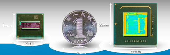
The Intel Atom processor (left) vs. The Poulsbo chipset (right)
With Poulsbo being a 130nm part, it also helps explain why Atom is reserved for larger-than-iPhone devices today: the pair of chips simply wouldn't fit in anything too small. There are obvious power consumption concerns as well, but physically getting these two into a smartphone-sized device is going to be impossible until the next iteration.
At a high level, Poulsbo looks to be no different than your run of the mill Intel chipset with integrated graphics:
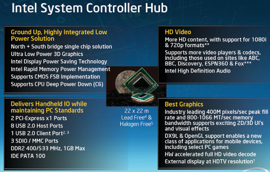
You'll quickly notice that the single chip solution, what Intel is calling a System Controller Hub (SCH) is a bit more unique. Instead of re-using a desktop chipset, Intel architected Poulsbo from scratch. In order to conserve power things like SATA and some of the USB ports were ripped out of the design. The designers chose to move back to PATA mostly because of power and smaller drives. Apparently in an idle state there isn't a power difference between PATA and SATA, but when actively transferring data SATA consumes much higher power due to its serial nature.
The FSB and memory frequencies are locked together which reduces power and PLL count. The chipset features a single channel DDR2-400/533 memory controller.
Poulsbo supports HD audio (Azalia, not the HD audio codecs) but reduced the number of audio engines supported in order to keep power under control. Only 2 channel audio is supported but you can access the audio interface externally, so conceivably you could dock an Atom device (such as a MID) and using an external codec get full 7.1 support.
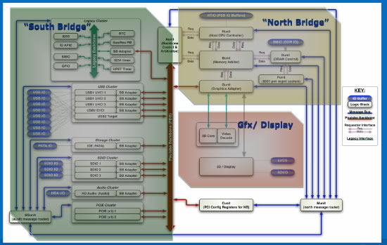
The parts of Poulsbo
Intel also developed a fairly sophisticated message fabric to send data across the SCH - think of it as an on-chip Ethernet network for carrying things like interrupts and power management signals across the chip in an efficient manner.
Poulsbo introduces a new FSB to memory bridge that's much simpler than conventional designs. In most chipsets you have many different queues for traffic between the FSB and memory subsystem designed to extract the best possible performance from the platform. With Poulsbo the designers simply outfitted the memory controller with a large 8K memory and all FSB/memory traffic must go through that. The single memory storage made validation a lot easier, the chipset itself a lot smaller but could incur a performance hit. The MCH/North Bridge part of the SCH is around 20% of the area of what traditional MCH/North Bridges are thanks to this approach.
The ICH/South Bridge parts of Poulsbo are similarly trimmed. Years of legacy have been stripped out of the chipset, there's no parallel port, no floppy disk controller. In mainstream chipsets as long as someone is using the feature, it must be kept in play - the same wasn't true for Poulsbo. If the target market didn't need it, the feature wasn't going in the chipset.
The benefit of cutting the fat in Poulsbo is that the chipset was physically smaller with fewer gates, meaning lower leakage power.
In a highly atypical move for Intel, Poulsbo also supports non-standard 1.5V DDR2 memory. There's no official JEDEC spec for 1.5V DDR2 memory but many vendors have good enough modules that will work at 1.5V, so if an OEM wants to undervolt its memory the chipset will support it.
Much of the Poulsbo's design couldn't have been done had it not been for the Atom project. There are many revolutionary techniques at work within Poulsbo, it's a more modular design, a more efficient design and potentially holds the key to better chipset design in general - but none of these techniques were ever allowed to surface before.
Intel's chipset business is like a clock, every year a new platform is expected and some of the more revolutionary changes that could potentially interrupt the normal flow of things are generally frowned upon. Poulsbo, at least internally, broke down a lot of these barriers. While it's far from the highest performance chipset Intel has ever produced, Poulsbo requires roughly half the power of mainstream chipsets. Intel has been on an efficiency kick with its CPUs for a few years now, Poulsbo may help ignite a similar trend with chipsets as well.


46 Comments
View All Comments
highlandsun - Thursday, April 3, 2008 - link
With all due respect to Fred Weber, with Atom at 47 million transistors, it's pretty obvious that the 10% figure for X86 ISA compatibility is not negligible, particularly in this performance-at-absolute-minimum-power space. Anybody using X86 in tiny embedded systems is automatically giving up a chunk of their power budget that someone using a cleaner instruction set encoding can apply directly to useful work. And as the previous poster already pointed out - source code portability is the only thing that matters to application developers, and that's a non-problem these days. Using the X86 instruction set encoding is stupid. Using it on a low-power-budget device is suicide.Jovec - Thursday, April 3, 2008 - link
I don't think the 10% reference meant 10% of all chips, but rather 10% of the current chip at the time the statement was made. In other words, x86 instruction decoding requires (roughly) a fixed amount of transistors for any chip, so the smaller the die size and larger the transistor count, less and less space is devoted to it.highlandsun - Thursday, April 3, 2008 - link
Yes, that's obvious. And it's also obvious that Atom at 47 million transistors is paying a greater proportionate cost than Core2 Duo at 410 million transistors. In 2002 when Fred made that statement, AMD's current chip was the AthlonXP Thoroughbred, with about 37 million transistors. At the same time the Pentium 4 had 55 million. Put in context, I'd guess that the Atom at 47M vs P4 at 55M has more than 10% of its resources devoted to X86 decoding.Also, Fred's statement in 2002 didn't take into account the additional complexity introduced by the AMD64 instruction extensions, where now a single instruction may be anywhere from 1 to 16 bytes long. Given that you're doing a completely clean ground-up chip design in the first place, it would have made more sense (from both a power budget and real estate perspective) to design a clean, orthogonal, uniform-length encoding at the same time.
Cross-platform ABI compatibility is stupid in the context they're aiming for; nobody is going to run their PC version of Crysis or MSWord on their cellphone. All that matters is API compatibility. With a consistent API, you can still run a separate binary translator if you really really want to move a desktop app to your mobile device but in most cases it would be a bad idea because a desktop app is unlikely to take advantage of power-saving APIs that would be important on a mobile. I.e., most of the time you're going to want purpose-built mobile apps anyway.
floxem - Tuesday, April 15, 2008 - link
I agree. But it's Intel. What do you expect?maree - Thursday, April 3, 2008 - link
I dont think MS will be ready before Windows 7 is released, which is another 3-5 years... and might coincide with Moorestown. Microsoft started work on WindowsLite only after releasing Vista. Vista is bloatware as of now. As of now MS has to rely on crippled versions of XP and Vista like starter and home, which is not very ideal.Apple and Linux are going to have a free run till then...
TA152H - Wednesday, April 2, 2008 - link
Bringing up the Pentium is a little strange, because the whole market is completely different.The Pentium wasn't supposed to be for everyone when it came out. The processor market was different back then where previous generations lasted a long, long time. The Pentium wasn't supposed to replace the 486 right away, or even quickly, and being huge and a terrible power hog was acceptable because the initial iteration was just for a very small group of people who absolutely needed it. The original Pentium had a lot of problems, and struggled badly to reach 66 MHz, so they sold most of their processors at 60 MHz. The second generation was intended more for mainstream.
Nowadays the latest generation replaces the earlier much more quickly, and has to cover more market segments more quickly. I still remember IBM releasing new machines for the 8086 in 1987. That's 9 years after the chip was made. It's just a different market.
The Pentium is nothing like the Silverthorne though, and it's a strange comparison. The Pentium executed x86 instructions, it wasn't decoupled. It also had both pipes, the U and V, lockstepped, which is limitation the Silverthorne doesn't have.
Saying the Pentium Pro was the first processor that allowed out of order processing is strange indeed. The only other processor this would have made sense with was the Pentium, since it was the only previous processor that was superscalar. So, they only made one in order processor, and then went to out of order with the next. It's difficult to see the extrapolation from this that it will be five years or more before Silverthorne goes out of order. It might be that long, but the backwards reference shouldn't be used to back that; it does more to contradict it.
Anand Lal Shimpi - Wednesday, April 2, 2008 - link
The Pentium reference was merely to show that what was once a huge, 300mm^2 design could now be built on a much, much smaller scale. And starting from scratch it's now possible to build something in-order that's significantly faster.The Pentium was an obvious comparison given that it was Intel's last two-issue in-order design, but I didn't mean to imply anything beyond that.
It won't be too long before we'll be able to have something the speed of a Core 2 in a similarly small/cool running package as well :)
Take care,
Anand
fitten - Wednesday, April 2, 2008 - link
I remember back in the days of the Mac FX we talked about 'what ifs' like making a 6502 with the (then) modern process technologies and how fast would it run. I wonder what about now :)crimson117 - Wednesday, April 2, 2008 - link
I am SO going to hold you to that! But I can only hope "won't be long" will mean within 12 months rather than within 12 years :P
Especially after my fiasco mounting a Freezer 7 Pro on an Abit IP35-E, I'd love if a heatsink weren't even necessary.
Anand Lal Shimpi - Wednesday, April 2, 2008 - link
12 months won't be a reality unfortunately :) But look at it this way, the first Pentium M came out in 2003? And 5 years later we're able to have somewhat comparable performance with the Atom processor.I'm really curious to see what happens with Atom on 32nm...