ASUS ROG Rampage Formula: Why we were wrong about the Intel X48
by Kris Boughton on January 25, 2008 4:30 AM EST- Posted in
- Motherboards
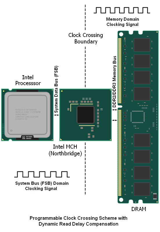
The Clock Crossing Procedure and MCH Read Delay (tRD)
Have you ever stopped to wonder how the Memory Control Hub (MCH) manages to transfer data from the system bus (FSB) to the memory bus and vice versa? Maybe you questioned why it was not possible to run your memory at any speed you desired, independent of the selected FSB. While there have been some chipsets that provide this capability, performance was rather spotty at times depending on the particular settings in use. In fact, these systems often resulted in the creation of rather large ranges of bus speed and memory speed ratios that refused to function, stable or otherwise. The concept was certainly fair enough, but at the time a well-engineered implementation turned out to be far more difficult that anyone may have been willing to concede. It should not come as a surprise that Intel chipsets have only allow the use of certain validated memory ratios - those same numbers we have grown to love (or hate) like 1:1, 5:4, 3:2, and so forth.
Back in the days of relatively slow-paced memory performance improvements, Intel had no problems pumping out processors with default FSB values that made running memory at synchronous speeds an expensive proposition. Thus they created the "down" divider that allowed the memory subsystem to run at a bus speed below that of the system bus. This allowed for a period of innovation where processor bus architecture was able to improve without placing an undue burden on the memory industry to create reasonably priced modules capable of these increased speeds.
In a lot of ways this also prevented cost-prohibitive aspects of validating higher data transfer rates from ultimately affecting the market as a whole. Because Intel was not obligated to allocate additional funding for the completion of this expensive process, the savings (however small) could be passed on to the consumer. When coupled with the added benefit of allowing for the purchase and use of lower-binned memory, we can easily see why a move such as this helped stimulate the industry into a period of unprecedented growth.
Today's market is much different. Older signaling technologies like Advanced Gunning Transceiver Logic (AGTL+), used almost exclusively by Intel in their monolithic CPU-to-MCH interface architecture, have just about reached the practical limits. As such, "up" dividers, those that allow for memory bus speeds in excess of the system bus speed, are used almost exclusively by high-performance systems. Indeed, it would be hard to imagine ever being satisfied with a system able to make use of memory operating at transfer rates of up to DDR2-667, and no higher. As odd as it may seem, the next generation of memory (DDR3) is based entirely on the concept of running at speeds mandating the use of at least a 2:1 memory bus to system bus frequency ratio.
When examined from this aspect it becomes clear what DDR3 really is - an early look at the next generation's mainstream memory component. Only when Intel has removed the performance barrier of their antiquated FSB and loosely-coupled MCH will we be fully able to finally experience the real improvements that DDR3 promises to provide. But we digress - speculating about what could have been done better or things to come is trite. Instead, let's concentrate on what can be done now to improve the collective performance of our systems.
Below is a somewhat basic representation of the problem at hand (and later we will introduce the fairly elegant solution that Intel has crafted in order to tackle said problem). Are you still wondering what the problem is? Put briefly: designing an effective means for transferring data from one bus "domain" to the other, while still respecting the timing requirements for each bus.
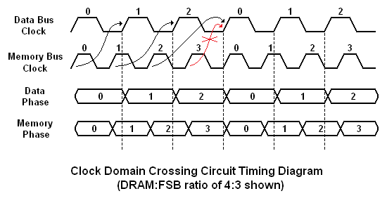
We made mention earlier that we believe Intel's solution to be quite elegant. While this is true, the system is still far from perfect as it introduces a significant amount of extra data access latency to each and every memory read request. It might seem ironic that the design initially constructed in order to allow for higher memory speeds ends up being the very reason for the additional latency penalty incurred, but this is the case. Coincidentally, we can apply a similar accounting of the system's flaws when explaining why actualized system performance improvements are always far less than predicted when making use of the larger dividers.
Moving data between two simultaneously running parallel buses requires a fine level of timing control and a fair amount of programmable logic to be successful, especially if the scheme is to remain flexible. The graphic below should help to illustrate the concept. Four memory data clock cycles for every three system data bus cycles (a 4:3 DRAM:FSB memory ratio) means that the MCH can do little more than queue up data requested from the memory for transport to the system bus.
This process works to ensure that no FSB cycles are left unused, but it does little to improve actual memory throughput. Because of this, the gains seen are largely due to the increased transfer efficiency. For the same reason, sustained data rates, while improved, are made at the expense of requiring added latency associated with the transfer scheme. This has the affect of retarding the responsiveness of short bursts of random read activity. Some users [Ed: Androids in disguise?] even swear that they can tell when they are using an Intel system because of the suppression of the "snappy" experience that comes when using true low-latency systems.
In order to better quantify exactly how the MCH clock crossing procedure influences system performance, it might be helpful to take a step back and examine the different component parameters that contribute to a system's overall memory read (access) latency. The diagram below helps to illustrate just this point - we have identified each distinct operation that takes place during a CPU data request and the sum of the individual latencies that involved with each part of the process make up the total system memory access latency, as measured. As we will see, this time - expressed in nanoseconds (ns) - is critical to overall system performance.
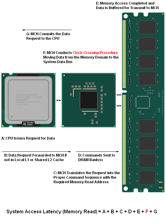
Although the user has at least minor control over just about every aspect of the system as modeled above, there are a few settings that when altered have the potential to drastically impact performance for the better (or worse, depending on how well you understand what you are doing). One of the most well known is the selection of primary memory timings (tCL-tRCD-tRP-tRAS). You may be surprised to learn that the effect of properly setting these values, represented by part "E", is quite insignificant when compared to your choice of tRD (the singular consideration in developing the latency associated with part "F"). This will be our focus for the remainder of our discussion. We have already lightly touched on this mysterious setting on the prior page.


73 Comments
View All Comments
poohbear - Friday, January 25, 2008 - link
one thing i liked about some of the recent high end mobo releases was the inclusion of an onboard wi-fi chip on a desktop mobo, but this mobo seems to be lacking that. i mean, they threw in everything but the kitchen sink, why not include wi-fi?:(TheDoc9 - Friday, January 25, 2008 - link
One of the best I've read here, definitely one of the best on over clocking I've ever read. It takes it to the next level, reminded me of how a body builder friend of mine schedules and calculates his workouts, calories, and entire life to be the best he can be. Hope to see more like this one in the future.jimru22 - Friday, January 25, 2008 - link
The article references the use of an Intel Extreme processor with adjustable multiplier. I'm planning on building a system hopefully anchored by the Asus Rampage Formula and a Intel Q9450 with locked 8X multiplier. Based in the charts, it seems to me that in order to run the Q9450 (333 MHZ) at 3.6 MHZ a 450 MHZ FSB is required. Therefore in this case, a tRD of 6 / Trd 13.3ns is the optimum value. Is this correct?kjboughton - Friday, January 25, 2008 - link
You would be correct. Processors with lower maximum multipliers present somewhat of a challenge when selecting the best memory configuration. In this case the 8x multiplier forces a higher than normally desired FSB, which is one of the many benefits of owning an Extreme processor (no such limitation). As such, the next best option, and the first choice for you, would be to go to 450MHz FSB and set a tRD of 6. Although this might not be completely ideal (we like to stick with 400MHz) your results will without a doubt be within a few percent of real-world performance at 400MHz FSB and a tRD of 5. Yet another reason why the Extreme line of processors are worth their price.Odeen - Saturday, January 26, 2008 - link
I'd like to differ on that.. As someone who first discovered overclocking during the Celeron 300A days, where a budget chip could run at 50-60% faster than its stock speed, and deliver higher performance than a $400 (at release time) Pentium III 450MHz, all without overstressing the rest of the platform (i.e. with bog-standard FSB and memory speed) I view overclocking as two ratios:Maximum attainable clock speed / original clock speed. 3:2 is the minimum ratio that isn't depressing to see booting up.
Cost of equivalent performance from a processor w/o overclocking / cost of actual processor. In the case the ratio was 4:1. Some of the best-case scenarios (like the very last 300A's being 100% overclockable to 600mhz), the ratio can be 6-7:1.
The Black Edition CPU's fail both value tests tests, because they are typically ONLY available at the fastest speed grades. Therefore, they are unlikely to reach a 30% overlock, never mind the requisite 50. And, being the most expensive SKU in the class combined with the lackluster overclock potential means that they are unlikely to outperform a processor that costs 4x as much (even an imaginary SKU that fits on the price-performance regression line of the class).
That said, if the Wolfdale E8190 is $130 and Intel somehow offers an "enthusiast edition" of it for $180 (that is, an edition for true enthusiasts, who want to extract the maximum bang for their buck), I would get one - the unlocked multiplier would make overclocking less of a "platform" issue (i.e. "how fast will the chip go until my motherboard peters out") and more of "how fast will this particular chip go period". I can definitely get behind that.
jimru22 - Friday, January 25, 2008 - link
Thank you Kris for the outstanding article as well as your response.Kind regards,
Jim
Orthogonal - Friday, January 25, 2008 - link
What are the chances someone could whip up an Excel Macro to incorporate all these inputs, equations and graphs for easy computation of optimal settings for a given CPU and Memory configuration.kjboughton - Friday, January 25, 2008 - link
Already exists, although you'll have to sweet-talk me into releasing the file. Seriously though, the Excel spreadsheet makes choosing the right settings downright simple.Orthogonal - Friday, January 25, 2008 - link
Fair enough, pretty please!Well maybe there could atleast be a web applet on the site or something of the sort. That would be killer.
LoneWolf15 - Friday, January 25, 2008 - link
Just one thought...IMO, no "Board Layout" portion of a review is complete without a picture of the port cluster on the back of the board.