ASUS ROG Rampage Formula: Why we were wrong about the Intel X48
by Kris Boughton on January 25, 2008 4:30 AM EST- Posted in
- Motherboards
MCH Read Delay Scaling and Default tRD Settings for Each Strap
Earlier, when we introduced the concept of the memory strap, we also included a table of common memory configurations that contained a column of "Default tRD" values. It's important to realize that these values are associated with the strap and have nothing to do with the actual FSB setting. This is because default operation assumes no overclocking, therefore if the 266 strap is being used then the processor obviously must be running at its rated FSB speed of 266MHz. Adding to this the element of a fully adjustable FSB introduces a new level of complexity that the system was never designed to handle.
This allows us to explain why making use of lower strap settings at one time provided for higher levels of performance - we've created the table below for just this purpose. (We say "at one time" because, as we will soon learn, most motherboards now implement strap changes in a manner much different than was previously done.) For example, selecting the 400 strap and setting a 1:1 memory divider at 400MHz FSB would result in DDR2-800 memory speed. By converting the FSB frequency into a cycle period (time for each clock tick) and then multiplying this value by the strap's default MCH Read Delay (tRD) we can effortlessly calculate the true latency (in nanoseconds) associated with this setting. As an example, dividing 1000 by the FSB (400MHz) gives us 2.5 (nanoseconds) - the co-efficient of 1000 used in this conversion formula was purposefully selected in order to give our result in the proper units. So, 12 times 2.5ns equals 30ns, which we then pair with our derived DDR speed rating of DDR2-800.
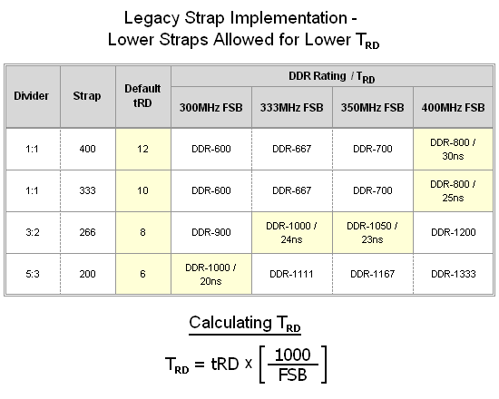
We will go into more detail about what this value means, but for the time being simply recognize that we want to minimize this number. We can see that the optimal configuration is one in which we would make use of a lower strap along with a higher FSB. While simultaneously applying these two considerations is obviously paramount in order to take advantage of this affect, the practical application of this approach is bounded in a number of ways. For instance, the near absolute minimum limit on any true read delay latency (tRD) might eventually come into play. We also need to be mindful of which memory dividers are available for the strap of choice, as these will ultimately dictate what final memory speeds are possible. Finally, we will soon learn that there are some strict rules that define whether or not a particular MCH Read Delay (tRD) is allowable, depending on the FSB, memory divider in use, and even the memory Column Address Strobe (CAS) setting.
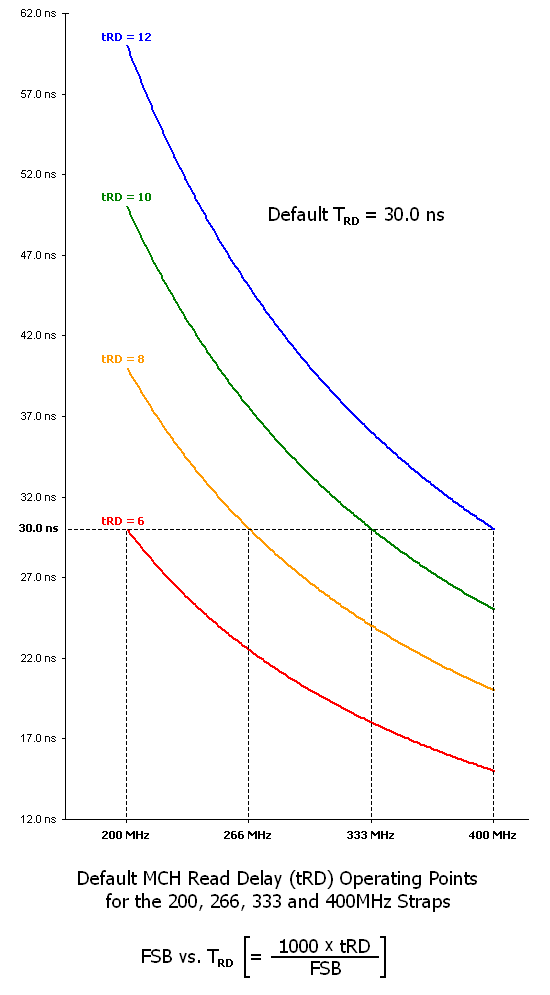
Now that we have had a chance to apply the simple equation to convert a tRD value into a TRD latency, we are ready to examine a graphic that displays the full breadth of this concept. We have plotted the complete range of FSB speeds encompassed by currently defined straps versus the derived TRD values for each default tRD associated with each strap. That may sound more complicated that what it really is; basically, these lines represent how TRD scales across our FSB window of interest (266 to 400MHz FSB) for each tRD in the table above. We can see that by drawing a vertical line from each default FSB up to the line corresponding to that strap's default tRD, and then reading across always results in the same TRD - 30.0 ns. This is by design, and is precisely how each default tRD was determined for all of the straps we have examined. It may be helpful to think of tRD as another memory timing, except that it has nothing to do with memory and everything to do with the MCH. In this sense it responds to FSB scaling in the same way as other memory timings - CAS (tCL), RAS to CAS (tRCD), Row Precharge (tRP) - the true latency (TRD) always decreases in a manner inversely proportional to FSB, and at some point will reach a minimum where the next higher tRD must be used in order to continue scaling.
What happens if we can set the tRD independent of the strap in use? Of course, the strap selected would still dictate which memory dividers are available, but no longer are we forced to make this change solely for the purposes of modifying tRD. As it turns out, this is exactly how these settings work with most of today's enthusiast motherboards built for overclocking, and the ASUS Rampage Formula is no exception. The ability to set a tRD value, regardless of the strap (i.e. memory divider), allows for a whole new world of possibilities when tuning for enhanced performance.
This brings us to the focus of true improvements made to the X38 chipset, which can be experienced more easily with X48 now. Too many benchmark reviews have been guilty of inappropriately discounting the value of this new chipset by calling the X48 little more than a "speed binned" version of the X38 and then comparing their relative performance at stock speeds. This would be like calling the QX6850 (3.00GHz default clock) a speed binned version of the Q6600 (2.4GHz default clock), benching them head-to-head at an equivalent speed, and then concluding that the QX6850 provides no additional value. Overclocking headroom is exactly what differentiates Intel's current line of Core 2 Extreme CPUs from their mainstream offerings, and it's also what makes the X48 stand head and shoulders above the X38 now that the BIOS designs have matured. When all is said and done, this just makes us wonder who really understands how to overclock the MCH properly.
MCH overclocking takes many forms. One form is something you might already be familiar with, carried out by simply raising the FSB. The problem is that BIOS setup routines will usually provide relief to the MCH by automatically relaxing tRD as the FSB is pushed higher and higher. This effect can easily negate any gains that might otherwise be achieved. Taking control of tRD and manually steering it to a lower value will allow the user to retain the associated performance increase, and as such must also technically be considered overclocking. As with most if not all positive performance adjustments realized while overclocking, this modification comes at a cost - in particular, the need for increased vMCH.
That is not to say that a certain level of headroom does not already exist as an accessible performance boost - it does. While Intel is wise to provide generous levels of margin between pre-established default tRD values and those attainable without the need for any additional voltage, we would consider ourselves foolish if we did not take advantage of this relatively free performance improvement. For instance, looking at the plot of X48 MCH overclocking response curves below we can see that although a default tRD value of 12 is normally used at greater than 400MHz FSB (using the 400 strap), at about 425MHz FSB we should have little to no trouble setting a tRD of 6, even using stock vMCH. The end result this tRD reduction of 6 clocks brings is a total memory read latency decrease of approximately 14.1ns (the difference in TRD values at 425MHz FSB using a tRD of 12 and 6).
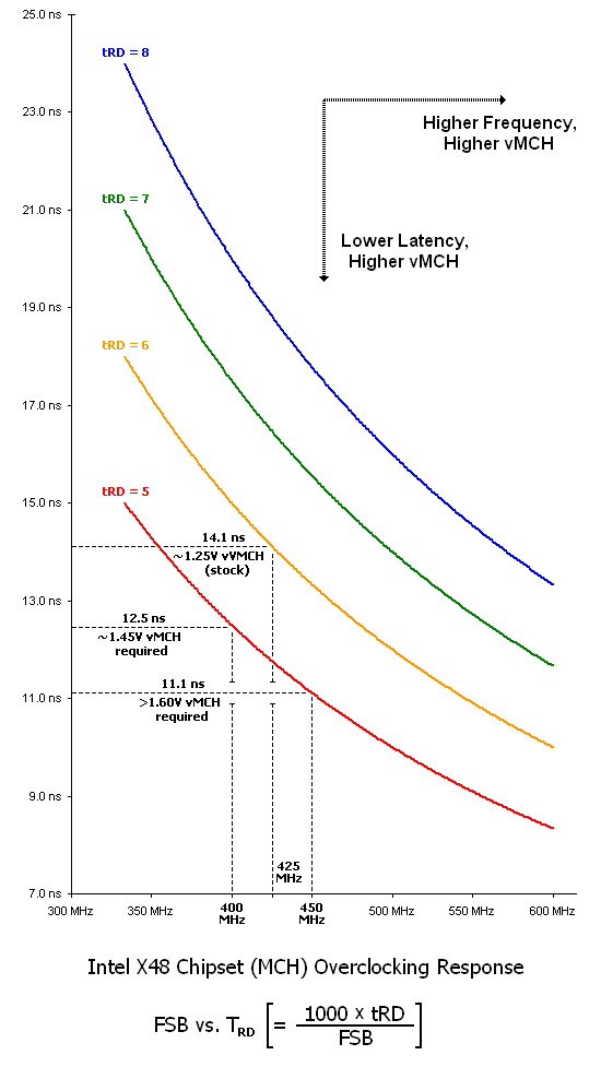
With that, we can finally see how this consideration comes full circle - the lower the TRD, the higher the memory read performance and vice versa. This change in TRD also drives vMCH, with lower values requiring substantially more voltage than the more "relaxed" (higher) values. We were able to push our ASUS Rampage Formula to a very impressive 450MHz FSB using a tRD of 5, which correlates to a TRD of about 11.1 ns. Because this required about 1.60V vMCH, for all intents and purposes we would consider this to be the practical limit of scaling, at least with conventional cooling. Above this voltage, we find that the X48 quickly turns into a little furnace during periods of prolonged load. Our recommendation is the liberal use of extra cooling capacity if you feel the need to push any further.


73 Comments
View All Comments
Orthogonal - Friday, January 25, 2008 - link
Just so I understand this correctly, due to the path the data and clocks must travel throughout the devices as explained on page 5, even though you can increase the bandwidth of the Memory modules, the MCH is ultimately the "bottleneck". Historically we falsely assumed higher bandwidth and lower CAS latency translated to better data throughput, but since tRD increased along with it, it was essentially wiped out or unused bandwidth. Now we try to lower tRD as low as possible to reduce MCH latency as it performs the "Clock crossing procedure", which is why the 400Mhz FSB with the lowest tRD latency gives the best data throughput.Also, does this mean that in your "Best Pick" DDR2 configuration summary that the two A+ choices highlighted in Green will effectively result in about the same performance since even though DDR2-1200 has more bandwidth than DDR2-1000, since the tRD=5, they will have the same Trd Delay (12.5ns).
Aivas47a - Friday, January 25, 2008 - link
I'm glad to see Asus implementing these new memory phase adjustment options in the bios. Now if they would provide a greater ability to fine-tune GTL reference voltages I would be a happy camper. GTL is a key setting for quad core overclocking success as Raja has helpfully explained in his DFI P35 review. The selectable percentages Asus currently provides are too crude and don't go high enough.mrlobber - Friday, January 25, 2008 - link
FCG, your article just flat out rocks, thanks for this one, we needed it badly :)One question about the previous Asus boards: X38 and also P35, which lack the exact tRD manipulation, providing the Transaction Booster stuff instead. As far as I understand, your analysis about the default tRD values set by different default fsb and memory divider combinations could also be used to determine the starting tRD value at least for the X38 chipset as well in a pretty straightforward way, and from that point being able to offset the tRD with Transaction Booster up or down to control it as necessary? (P35 would have different default tRD's, but the underlying principles should stay the same?)
And, by making appropriate changes in x values if needed, your POST / no POST inequality should stay applicable as well, right?
kjboughton - Friday, January 25, 2008 - link
All true, although we did talk about how these straps at one time had default tRD values associated with them, the difference has become that these default values are now usually based on the real underlying requirements, such as FSB. Now, exactly how each motherboard vendor sets up and implements this value has a lot to do with how their motherboard falls out in comparison testing. With that being said, boards that perform better generally make use of lower tRD values by default. And because X48 is a speed-binned version of X38, which is superior to P35 with it comes to MCH overclocking, it is also safe to say that the higher-end chipsets will allower the same (or lower) tRD values at FSB levels where the other chipsets may fall flat on their faces. Make sense?Regarding the 'Test POST Equation' - absolutely, I know those equations to be true for X38/X48 but I wouldn't doubt if they ended up being exactly the same for say, P35. A little bit of testing should validate this assumption... ;)
Orthogonal - Friday, January 25, 2008 - link
Can we expect a similar analysis and optimization of strappings, timings etc... when an X48 DDR3 compatible board is released?kjboughton - Friday, January 25, 2008 - link
Yes, the will be an easy bridge to make. DDR3 is very similar to DDR2 and in a lot of respects is a simply extension of the logic already developed. In any case, we will provide this information for reference when the time comes.daddyo323 - Friday, January 25, 2008 - link
I've overclocked a couple cpus before, and each time, I had stability problems due to memory.I have built many systems, but since gave up on overclocking... these new Cores and chipsets look like they were made for it...
My question is, was that CPU stable at 4ghz, and could we have a chart on which settings to set, exactly... I wonder how far we can push this platform with the air cooling.
kjboughton - Friday, January 25, 2008 - link
Everything you want to know, about more, about this CPU can be seen here: http://www.anandtech.com/cpuchipsets/intel/showdoc...">http://www.anandtech.com/cpuchipsets/intel/showdoc...We used the same CPU that can be read about in the above review. The short answer is yes, we were completely stable at 4GHz with just 1.28V real under load.
Cheers,
Kris
Quiksilver - Friday, January 25, 2008 - link
Has there been an ETA on the release date of the X48 chipset? I thought they were supposed to come out in December but they never appeared and this would be the second X48 preview I've seen for AT. Also I remember seeing a flow chart somewhere that had DDR2 & DDR3 being the differences between X38 and X48 of which X38 had both but now it seems X48 has DDR2 as well but will the DDR2 boards be available at launch or are they coming later on?Gary Key - Friday, January 25, 2008 - link
ASUS is telling us mid-February for the X48 launch now. Gigabyte and MSI have confirmed that also, but we have had dates confirmed about a dozen times over the last two months and it always seems to change about three days before the next "official" launch. ;)