ASUS ROG Rampage Formula: Why we were wrong about the Intel X48
by Kris Boughton on January 25, 2008 4:30 AM EST- Posted in
- Motherboards
The Clock Crossing Procedure and MCH Read Delay (tRD)
Have you ever stopped to wonder how the Memory Control Hub (MCH) manages to transfer data from the system bus (FSB) to the memory bus and vice versa? Maybe you questioned why it was not possible to run your memory at any speed you desired, independent of the selected FSB. While there have been some chipsets that provide this capability, performance was rather spotty at times depending on the particular settings in use. In fact, these systems often resulted in the creation of rather large ranges of bus speed and memory speed ratios that refused to function, stable or otherwise. The concept was certainly fair enough, but at the time a well-engineered implementation turned out to be far more difficult that anyone may have been willing to concede. It should not come as a surprise that Intel chipsets have only allow the use of certain validated memory ratios - those same numbers we have grown to love (or hate) like 1:1, 5:4, 3:2, and so forth.
Back in the days of relatively slow-paced memory performance improvements, Intel had no problems pumping out processors with default FSB values that made running memory at synchronous speeds an expensive proposition. Thus they created the "down" divider that allowed the memory subsystem to run at a bus speed below that of the system bus. This allowed for a period of innovation where processor bus architecture was able to improve without placing an undue burden on the memory industry to create reasonably priced modules capable of these increased speeds.
In a lot of ways this also prevented cost-prohibitive aspects of validating higher data transfer rates from ultimately affecting the market as a whole. Because Intel was not obligated to allocate additional funding for the completion of this expensive process, the savings (however small) could be passed on to the consumer. When coupled with the added benefit of allowing for the purchase and use of lower-binned memory, we can easily see why a move such as this helped stimulate the industry into a period of unprecedented growth.
Today's market is much different. Older signaling technologies like Advanced Gunning Transceiver Logic (AGTL+), used almost exclusively by Intel in their monolithic CPU-to-MCH interface architecture, have just about reached the practical limits. As such, "up" dividers, those that allow for memory bus speeds in excess of the system bus speed, are used almost exclusively by high-performance systems. Indeed, it would be hard to imagine ever being satisfied with a system able to make use of memory operating at transfer rates of up to DDR2-667, and no higher. As odd as it may seem, the next generation of memory (DDR3) is based entirely on the concept of running at speeds mandating the use of at least a 2:1 memory bus to system bus frequency ratio.
When examined from this aspect it becomes clear what DDR3 really is - an early look at the next generation's mainstream memory component. Only when Intel has removed the performance barrier of their antiquated FSB and loosely-coupled MCH will we be fully able to finally experience the real improvements that DDR3 promises to provide. But we digress - speculating about what could have been done better or things to come is trite. Instead, let's concentrate on what can be done now to improve the collective performance of our systems.
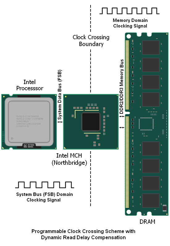
Below is a somewhat basic representation of the problem at hand (and later we will introduce the fairly elegant solution that Intel has crafted in order to tackle said problem). Are you still wondering what the problem is? Put briefly: designing an effective means for transferring data from one bus "domain" to the other, while still respecting the timing requirements for each bus.
We made mention earlier that we believe Intel's solution to be quite elegant. While this is true, the system is still far from perfect as it introduces a significant amount of extra data access latency to each and every memory read request. It might seem ironic that the design initially constructed in order to allow for higher memory speeds ends up being the very reason for the additional latency penalty incurred, but this is the case. Coincidentally, we can apply a similar accounting of the system's flaws when explaining why actualized system performance improvements are always far less than predicted when making use of the larger dividers.
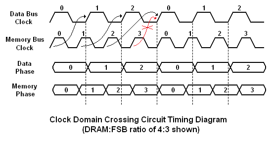
Moving data between two simultaneously running parallel buses requires a fine level of timing control and a fair amount of programmable logic to be successful, especially if the scheme is to remain flexible. The graphic below should help to illustrate the concept. Four memory data clock cycles for every three system data bus cycles (a 4:3 DRAM:FSB memory ratio) means that the MCH can do little more than queue up data requested from the memory for transport to the system bus.
This process works to ensure that no FSB cycles are left unused, but it does little to improve actual memory throughput. Because of this, the gains seen are largely due to the increased transfer efficiency. For the same reason, sustained data rates, while improved, are made at the expense of requiring added latency associated with the transfer scheme. This has the affect of retarding the responsiveness of short bursts of random read activity. Some users [Ed: Androids in disguise?] even swear that they can tell when they are using an Intel system because of the suppression of the "snappy" experience that comes when using true low-latency systems.
In order to better quantify exactly how the MCH clock crossing procedure influences system performance, it might be helpful to take a step back and examine the different component parameters that contribute to a system's overall memory read (access) latency. The diagram below helps to illustrate just this point - we have identified each distinct operation that takes place during a CPU data request and the sum of the individual latencies that involved with each part of the process make up the total system memory access latency, as measured. As we will see, this time - expressed in nanoseconds (ns) - is critical to overall system performance.
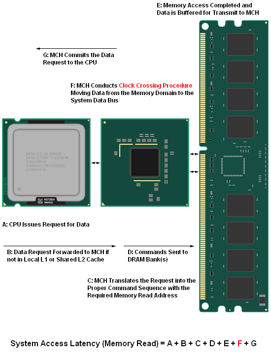
Although the user has at least minor control over just about every aspect of the system as modeled above, there are a few settings that when altered have the potential to drastically impact performance for the better (or worse, depending on how well you understand what you are doing). One of the most well known is the selection of primary memory timings (tCL-tRCD-tRP-tRAS). You may be surprised to learn that the effect of properly setting these values, represented by part "E", is quite insignificant when compared to your choice of tRD (the singular consideration in developing the latency associated with part "F"). This will be our focus for the remainder of our discussion. We have already lightly touched on this mysterious setting on the prior page.


73 Comments
View All Comments
Orthogonal - Friday, January 25, 2008 - link
Just so I understand this correctly, due to the path the data and clocks must travel throughout the devices as explained on page 5, even though you can increase the bandwidth of the Memory modules, the MCH is ultimately the "bottleneck". Historically we falsely assumed higher bandwidth and lower CAS latency translated to better data throughput, but since tRD increased along with it, it was essentially wiped out or unused bandwidth. Now we try to lower tRD as low as possible to reduce MCH latency as it performs the "Clock crossing procedure", which is why the 400Mhz FSB with the lowest tRD latency gives the best data throughput.Also, does this mean that in your "Best Pick" DDR2 configuration summary that the two A+ choices highlighted in Green will effectively result in about the same performance since even though DDR2-1200 has more bandwidth than DDR2-1000, since the tRD=5, they will have the same Trd Delay (12.5ns).
Aivas47a - Friday, January 25, 2008 - link
I'm glad to see Asus implementing these new memory phase adjustment options in the bios. Now if they would provide a greater ability to fine-tune GTL reference voltages I would be a happy camper. GTL is a key setting for quad core overclocking success as Raja has helpfully explained in his DFI P35 review. The selectable percentages Asus currently provides are too crude and don't go high enough.mrlobber - Friday, January 25, 2008 - link
FCG, your article just flat out rocks, thanks for this one, we needed it badly :)One question about the previous Asus boards: X38 and also P35, which lack the exact tRD manipulation, providing the Transaction Booster stuff instead. As far as I understand, your analysis about the default tRD values set by different default fsb and memory divider combinations could also be used to determine the starting tRD value at least for the X38 chipset as well in a pretty straightforward way, and from that point being able to offset the tRD with Transaction Booster up or down to control it as necessary? (P35 would have different default tRD's, but the underlying principles should stay the same?)
And, by making appropriate changes in x values if needed, your POST / no POST inequality should stay applicable as well, right?
kjboughton - Friday, January 25, 2008 - link
All true, although we did talk about how these straps at one time had default tRD values associated with them, the difference has become that these default values are now usually based on the real underlying requirements, such as FSB. Now, exactly how each motherboard vendor sets up and implements this value has a lot to do with how their motherboard falls out in comparison testing. With that being said, boards that perform better generally make use of lower tRD values by default. And because X48 is a speed-binned version of X38, which is superior to P35 with it comes to MCH overclocking, it is also safe to say that the higher-end chipsets will allower the same (or lower) tRD values at FSB levels where the other chipsets may fall flat on their faces. Make sense?Regarding the 'Test POST Equation' - absolutely, I know those equations to be true for X38/X48 but I wouldn't doubt if they ended up being exactly the same for say, P35. A little bit of testing should validate this assumption... ;)
Orthogonal - Friday, January 25, 2008 - link
Can we expect a similar analysis and optimization of strappings, timings etc... when an X48 DDR3 compatible board is released?kjboughton - Friday, January 25, 2008 - link
Yes, the will be an easy bridge to make. DDR3 is very similar to DDR2 and in a lot of respects is a simply extension of the logic already developed. In any case, we will provide this information for reference when the time comes.daddyo323 - Friday, January 25, 2008 - link
I've overclocked a couple cpus before, and each time, I had stability problems due to memory.I have built many systems, but since gave up on overclocking... these new Cores and chipsets look like they were made for it...
My question is, was that CPU stable at 4ghz, and could we have a chart on which settings to set, exactly... I wonder how far we can push this platform with the air cooling.
kjboughton - Friday, January 25, 2008 - link
Everything you want to know, about more, about this CPU can be seen here: http://www.anandtech.com/cpuchipsets/intel/showdoc...">http://www.anandtech.com/cpuchipsets/intel/showdoc...We used the same CPU that can be read about in the above review. The short answer is yes, we were completely stable at 4GHz with just 1.28V real under load.
Cheers,
Kris
Quiksilver - Friday, January 25, 2008 - link
Has there been an ETA on the release date of the X48 chipset? I thought they were supposed to come out in December but they never appeared and this would be the second X48 preview I've seen for AT. Also I remember seeing a flow chart somewhere that had DDR2 & DDR3 being the differences between X38 and X48 of which X38 had both but now it seems X48 has DDR2 as well but will the DDR2 boards be available at launch or are they coming later on?Gary Key - Friday, January 25, 2008 - link
ASUS is telling us mid-February for the X48 launch now. Gigabyte and MSI have confirmed that also, but we have had dates confirmed about a dozen times over the last two months and it always seems to change about three days before the next "official" launch. ;)