ASUS ROG Rampage Formula: Why we were wrong about the Intel X48
by Kris Boughton on January 25, 2008 4:30 AM EST- Posted in
- Motherboards
The Basics of Strap Selections, Dividers and Derived Memory Speeds
We have discussed MCH Read Delay (tRD) and its effects on memory read performance before. About a year ago, this particular setting allowed some vendors to design boards that seemed to outperform competing companies' products consistently on a clock-for-clock basis. This was around the time that the enthusiast community first realized the importance of "straps". Some found that by setting a lower strap while running an equivalent Front Side Bus (FSB) that they were able to achieve better performance, higher frame rates, and better benchmark completion times all without the help of any additional tuning.
For those that are unfamiliar with what we mean by strap, consider the following example. Suppose you have two different CPUs, each with a different default FSB, as is the case with first-generation Core 2 processors (266MHz) and current 45nm Core 2 processors (333MHz). If you were to install these processors in identical systems each would be capable of running the same memory speeds (at least DDR2-667 and DDR2-800), regardless of the processor's default FSB. For the 266MHz default FSB processor, this would require a 5:4 and 3:2 divider respectively, while the 333MHz FSB variant would need 1:1 and 6:5. These ratios are necessary in order for the motherboard to set up allowable memory subsystem to system data bus interface configurations.
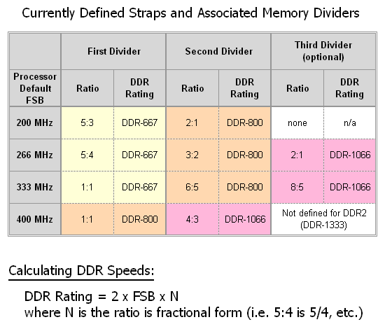
Because of this, the motherboard does not need to know anything about the installed processor and memory, other than the default FSB and the memory's SPD rating, which are both read programmatically prior to Power On Self Test (POST). For example, a 266 FSB processor paired with DDR2-800 memory will make use of the associated 266 strap's second divider - as would a 333 FSB processor. Would you be surprised to learn this works exactly the same way for a 200 FSB processor? Well, it does, and in fact it does not matter which processor type is installed - all combinations work and allow for the same exact memory speeds - DDR2-667 and DDR2-800 (and sometimes DDR2-1066).
If slower memory is detected the system simply uses the first divider in order to achieve DDR2-667 speeds. In the case of faster memory, the third divider is used for DDR2-1066 - which is sometimes available, depending on the strap in use. (All 266, 333, and the upcoming 400 MHz FSB parts will be able to make use of this new official memory speed, as recently announced by JEDEC.) One final note, "down" dividers are no longer possible with Intel platforms and as such the lowest supported memory speed for systems that will make use of the QX9770 (when it arrives) will be DDR2-800, unless the user chooses to underclock the FSB.
As we can see, this system allows for maximum component interchangeability and configuration flexibility all through the use of relatively straightforward selection logic. Check the table below for more information on how to derive these numbers.
Now that we know a little more about what straps are and how they work, we are ready to discuss what they mean when overclocking. Let's say you have an E6700 that makes use of a default FSB of 266MHz - pushing the FSB to 400 while making use of the processor's default strap's second divider (3:2) results in a final memory speed of DDR2-1200, a goal that might be outside the realm of normal achievement unless you have memory capable of this speed. By selecting the 400 strap the 1:1 and 4:3 dividers become available and we are able to set a more modest speed of either DDR2-800 or even DDR2-1066. Alternatively, choosing the 266 strap permits use of the 5:4 divider for DDR2-1000.
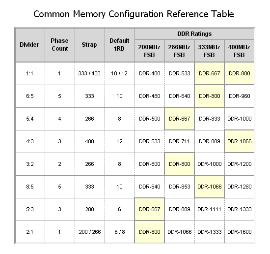
The point is that the freedom to choose any strap we want, regardless of CPU type installed, gives us the choice to make use of a whole myriad of memory speed settings that would otherwise be unavailable. Take note of the "Default tRD" column; you will see that each strap has an associated value (6 at the 200 strap, 8 for 266, etc.) We will discuss this particular setting in detail a little later.
Until now, choosing a memory divider in order to set a final memory speed was easy. Most users focus solely on achieving maximum CPU frequency, letting the memory speed fall where it will. Although it is possible for memory to be the limiting component when overclocking, this is unlikely considering the low cost and high availability of today's performance DDR2 modules. Thus it's easy to pick a memory divider that places the memory operating point near a maximum without ever considering what could be done in order to further improve performance.
Perhaps too many users feel the time they need to invest in fine-tuning their memory settings is not worth the effort. While this might not be far from the truth, we find this hard to believe. Major memory manufactures like OCZ, Corsair, Cell Shock, G.Skill, and Team Group have entire departments of support personnel that work hard every day to provide users the assistance they need to make the most of their purchase. These groups are inundated with requests for help, from both experienced users and novices alike.
Going back to what we said before, what does all of this have to do with better performance on a clock-for-clock basis? In a word: everything! We would like to provide some solid information on the subject as to why the age-old quest for maximum FSB is not always the best approach; in fact, it is often the wrong approach. Our hope is that once allowed an opportunity to make use of this information, users will begin to understand the true limitations of their system components better and might perhaps stop inappropriately blaming overclocking failures on perfectly good hardware. Better yet, they'll stop buying boards based solely on FSB capability when overall system performance is much more important.
Now that we have had a chance to review the basics on memory straps let's move on to something a little more interesting - MCH clock crossing operation and the associated MCH Read Delay (tRD).


73 Comments
View All Comments
dallas - Monday, March 24, 2008 - link
I was wondering how this chipset and Windows Vista 64-bit handles IRQ ? I have a Creative X-fi and it has had a lot of problems with PCI-latency and shared IRQ. According to the manual PCI slot 2 is the only one of the two that does not share IRQ with the graphic cards. Do you guys have any experience of this ?Second question is related also to IRQ. I have a Razer Deathadder mouse which I use at 1000Hz polling rate and it seems to cause quite a bit CPU-usage (average of 10% with AMD64 3500+ when moving mouse at desktop without overlapping anything). I guess it would be ideal to connect it to a USB-port not sharing any IRQ. Rampage Formula has 12 USB-ports total, but reading the manual it says there is USB controllers 1 to 6 and USB 2.0 controllers 1 and 2. How do I relate these figures to the actual layout of the board ? USB controllers 2 and 5 are the only ones not sharing IRQ.
http://dlsvr01.asus.com/pub/ASUS/mb/socket775/Ramp...">http://dlsvr01.asus.com/pub/ASUS/mb/soc...rmula/Ra...
Thanks
nitemareglitch - Friday, March 7, 2008 - link
My older DFI nForce 4 board had fully adjustable tRd among other things. Asus taking a play from their book?rge - Monday, February 18, 2008 - link
Granted I am using gigabyte p35 dq6 board, but I thought loadline simply was a sensor adjustment? Anyone know what is meant by induced power instabilities? measured by?I thought (and may well be wrong) that with loadline disabled, if I choose 1.25v bios as vcore, idle would be 1.23 volts (Voffset), load (dual core) would be 1.22v (Vdroop), when load stops, overshoot to 1.25v before decreasing back to 1.23 idle. Thus when you are choosing 1.25 volts in bios, you are choosing max volts ie, overshoot max, and not idle volts.
I thought loadline was simply a ~.02v sensor calibration, so when enabled, and you choose 1.25 volts in bios, you are then choosing the idle volts (instead of overshoot max) and thus it idles at 1.25V. During load you still see vdroop to 1.24v, and overshoots to 1.27v.
In other words no difference between loadline enabled 1.23v and loadline disabled 1.25v, just personal preference of making bios vcore set idle volts or max overshoot volts.
If I am wrong can someone please inform me what loadline is, and what is meant by power instabilities...mean ?greater fluctuations in volts or what?
Nickel020 - Saturday, February 16, 2008 - link
Firstly, great article! Got me a long way in increasing my memory speed and understanding the underlying factors.What I don't understand though is why the X48 is better than the X38. I already have the option to change tRD on my Gigabyte P35 DQ6, and I'm getting much better memory perfromance after manually setting it to 6.
As I see it, the option to adjust tRD is only a BIOS issue and it can be done on P35 and X38, so how does this make the X48 a better chipset?
kjboughton - Sunday, February 17, 2008 - link
The difference comes in the voltages required to run equivalent speeds/tRD settings. In fact, the X48 board are capable of running stable at much higher speeds, using tigher MCH Read Delay (tRD) values at lower voltages. More to come soon...Holmer - Monday, February 18, 2008 - link
Thanks for an excellent article.I would just love to know how well the Rampage formula handles overclocking with 4x1 GB RAM? How large is the performance hit as compared to 2x2 GB and can it handle 1200 MHz (with two 2x1 GB kits rated at this speed).
Roughly when can we expect the loon awaited X48 roundup?
Thanks a lot on beforehand.
Holmer - Friday, February 22, 2008 - link
Another question: Is is possible to manually set tRFC > 42 in BIOS? If yes what is the maximun value of tRFC?I would be very grateful for an answer.
The Ghost - Saturday, February 2, 2008 - link
With 400Mhz, tRD of 4, CL of 4 and 3:2 ratio I get this:1,334 > 1,333
Is that enough to post or is 0,001 to little to "allowed" ?
Vikendios - Wednesday, January 30, 2008 - link
It's all very fine, but as long as ATI/AMD GPU's are outclassed by Nvidia's, the gamer scene which drives the $300+ motherboard business has little interest in non-Nvidia-SLI solutions. It's bizarre that Intel focuses on chipsets that can apparently only handle well (correct me if I'm wrong) their arch-competitors AMD's GPU's in (Crossfire) arrays.Intel should hurry to develop competitors to 790i that are really neutral as to which twinned or tripled video cards are used.
Gary Key - Wednesday, January 30, 2008 - link
The last time I tested it, X38 ran SLI faster than 680i. The problem is not the chipset, it is simply a decision by NVIDIA (and/or Intel) not to "officially" license SLI on the Intel chipset platforms, except for the upcoming Skulltrail board.This whole SLI/Crossfire debate has gone on long enough, the technologies accomplish the same purpose (are practically identical from a technological viewpoint) and setting up a board/BIOS to run either is actually very easy. CF runs just fine on the NV680i/780i and SLI runs just fine on the 975X/X38/X48 if driver support is present and the proper switches are enabled in the BIOS. Personally, I would like to have the ability to run (unhindered) AMD or NVIDIA GPUs in multi-GPU configurations on either chipset platform. I just wish they would let the market determine the best multi-GPU solution, but that is pie in the sky thinking. ;)