PCI Express 2.0: Scalable Interconnect Technology, TNG
by Kris Boughton on January 5, 2008 2:00 AM EST- Posted in
- CPUs
PCI Express Link Speeds and Bandwidth Capabilities
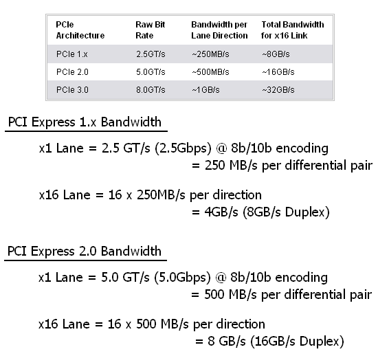
PCI Express uses a highly scalable architecture that is capable of delivering high bandwidth with a relatively low pin-count, dramatically simplifying design complexity while simultaneously allowing for smaller interface footprints. This is accomplished through the use of Low Voltage Differential Signal (LVDS) signal pairs - a simple two wire connection allowing for 1 bit to be transferred per clock (therefore 1GT/s is equal to 1Gbps). A pair per direction makes bi-directional signaling possible, which effectively doubles the throughput to 2 bits per cycle. Together these four pins comprise a single "lane." No additional pins are needed for data transfer as the clock signal is transmitted using these same pins through the use of an encoding scheme known as 8b/10b encoding. Without getting into too much detail this means that 8 bits of data are transferred using a 10-bit signal. While this does add 25% overhead to each data transfer, it eliminates the need to route separate traces for clock signals, the downside being that the maximum throughput is reduced by about 20%. Because the clock rate is so high (2.5GHz), the PCI Express protocol is able to transfer up to 500MB/s of bi-directional data with just four pins (compared to the legacy PCI bus which transfers 133MB/s of data using 32 pins). Higher data transfer rates require either the use of numerous parallel traces or increased clocking rates - in this case we can see that the tradeoff has been clearly been made in favor of a low-pin count.
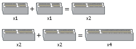
Multiple lanes can be grouped through a method knows as training, wherein the downstream device and the host negotiate how many lanes will be assigned. Although plugging a PCI Express card into a slot smaller than itself is not physically possible, plugging into a larger slot is mechanically possible. During training, the host device simply queries the device for its maximum link speed and assigns resources as needed. (Keep in mind that link speed is a bit of a misnomer - the PCI Express physical link layer always operates at the same frequency; it's the number of assigned lanes that changes). This method becomes a little more complicated in the case where the mechanical size of the slot does not necessarily match the host's maximum offered link speed. For example, many of today's X38-based motherboards include a third x16 slot but are only capable of providing x4 bandwidth (PCI Express 1.x) - more on why this is later. In this case, the installed device must be willing to operate at a reduced link speed. The PCI Express interface supports interconnect widths of x1, x2, x4, x8, x16, and x32. As an aside, PCI-E x32 slots are rarely seen because of their exceptional length, but thanks to PCI Express 2.0 we can now get the same bandwidth in PCI-E x16 form factor.
The part of the installed card's edge connector to the left of the key notch is always the same, no matter the card. Power, ground, reference voltages, and pads for control, training, and link maintenance are located here and are the required minimum required for operation. Data transfers to and from the device are accomplished using repeating blocks of pads - those that form the signals that comprise a single lane. The longer the slot is from the right of the keyway the higher the speed it offers (this assumes that it does in fact offer a maximum link speed congruent with its mechanical size). This all makes determining a device's default link speed quite easy - a quick look at the length of the edge connector and you have everything you need to know.
The table below compares PCI Express 1.x with 2.0 as well as 3.0 (which is now in the development stage - expect to see products based on this revision sometime in 2010). PCI Express 2.0 builds upon PCI Express 1.x primarily through the doubling of the clock rate to 5.0GHz (up from 2.5GHz). This brings to light an important point: earlier we noted that the PCI Express physical link layer always operates at the same speed. This is true except in the case where a PCI Express 1.x device is installed in a PCI Express 2.0 compliant slot - although the host is capable of the higher signaling frequency the device is not; the result being the use of the slower (2.5GT/s) clock rate. Note how the 8b/10b encoding overhead is factored into the actual usable bandwidth calculation.
Using PCI Express 2.0, motherboard designers can now either offer double the bandwidth in an equivalent size slot or can choose to create smaller layouts without sacrificing performance. In any case, this additional design flexibility paves the way for significant improvements in future products. PCI Express 3.0 will likely double the bandwidth provided by the previous generation again. You may have noticed though that the change must come from something more than just a decrease in the cycle time. This will be due a change in the encoding scheme - PCI-E 3.0 will stop using 8b/10b encoding, and whether or not the new scheme is truly more efficient than that used today remains to be seen. Expect the same level of backward-compatibility though as PCI-SIG is already assuring us that our then ancient PCI Express 1.x cards will run without difficulty in a PCI Express 3.0 slot. Let's take a closer look at exactly why they can make such a bold claim.


21 Comments
View All Comments
kjboughton - Sunday, January 6, 2008 - link
Are you sure this isn't fiber or optical? Any supporting information you can provide would be great.Hulk - Saturday, January 5, 2008 - link
First of all great article. Great writing. You should be proud of that article.I see that currently the Southbridge can transmit data to the Northbridge at 2GB/sec max. In real world situations about how much bandwidth would the Southbridge require assuming a light, medium, and heavy loading situation?
kjboughton - Monday, January 7, 2008 - link
I can help you with some of the base information needed to calculate this yourself (since every system is different based on attached peripherals as well as their type) and we'll leave the rest to you as an exercise.For example, a 1Gbps Ethernet connection to the ICH would have a maximum theoretical sustained data transfer rate of 125MB/s (1Gbps x 1 byte/8 bits). A single SATA 3.0Gbps drive would be limited by the interface to three times this number, or about 375MB/s (although the disk to bus/cache transfer rate is much less, somewhere on the order of 120-140MB/s sustained) - but nevertheless, burst read speeds could easily saturate the bus in one direction (1Gbps). Then there's USB devices, possibly a sound card or other onboard solution...going through the numbers, adding up the maximum possible bandwidth for all your attached devices you should be able to get an idea for what would be "light, medium and heavy" loading for your system. Again, this is something that varies from system to system. Hope this helps.
LTG - Saturday, January 5, 2008 - link
Excellent article, good tech level.Would you believe "simple ecards" benefit from PCI-E 2.0 right now?
At most sites when you send an ecard it just e-mails a link to a flash animation to someone.
However when you send an ecard at the site below, it's rendering and compositing custom photos and messages into a 3d scene on the fly for each card sent.
Because this is a web site all of this runs on the server side for many users at once.
PCI-E 3.0 will be welcome :).
http://www.hdgreetings.com/preview.aspx?name=count...">http://www.hdgreetings.com/preview.aspx?name=count...
or
www.hdgreetings.com (sorry, link buttons not working)
JarredWalton - Saturday, January 5, 2008 - link
I don't know that e-cards would really benefit much - especially right now. The FSB and memory bandwidth aren't much more than what an x16 PCI-E 2.0 slot can provide in one direction (8GB/s). I would imagine memory capacity and the storage subsystem - not to mention network bandwidth - are larger factors than the PCI-E bus.Are you affiliated with that site at all? If so, I'd be very interested to see a performance comparison with a single 8800 GTX vs. an 8800 GT on a PCI-E 2.0 capable motherboard. The 8800 GTX even has a memory and performance advantage, but if as you say the bottleneck is the PCI-E bus, it should still see a performance increase from the 8800 GT.
LTG - Sunday, January 6, 2008 - link
Hi Jared, yes I'm a developer on the site - (pls don't think of my post as spam, i've been a reader at AT forever and it just seemed relevant :)You could be right, we are just now starting to test pci2.0 so the benchmark you mention will definitely shed some light.
The network is not a bottleneck because cards are rendered and compressed on a given server node.
The disk IO is a 6 drive RAID0 array (no data is at risk because the nodes just render jobs) with the Segate 7200.11 drives max out at 100MB/sec transfer rate each, which is less than 600MB/sec total, however I have "heard" that the effective PCI-E video card bandwidth is much less than the theoretical limit.
I wish there were a utility to easily measure PCI-E bandwidth but currently I only know of indirect experiments as you mention.
Thanks again for the nice article.
PizzaPops - Saturday, January 5, 2008 - link
I can't help but be amazed by the speed at which hardware is improving. I remember when we were stuck with just PCI and AGP for what seemed like forever. Now the speeds are getting ridiculous. Can't wait to see what the future has in store.Very informative article and not too difficult for the average person to understand either. Now I know why my X38 gets so hot.
Spoelie - Saturday, January 5, 2008 - link
Why does the 790FX stays so cool then?Besides, there hasn't been a review of that one yet on AT.
Gary Key - Saturday, January 5, 2008 - link
The 790FX does not have the memory controller on-board among other items, so the additional power required for PCI-E 2.0 is minimal at best as are resulting thermal increases. AMD also took a very elegant approach on the 790FX in regards to PCI-E 2.0 (they had time to ensure proper integration, Intel's is fine, just they had a lot to cram into the chipset this time around ;) ) that we will cover shortly.NVIDIA's current approach on the 780i is to use a bridge chipset that is creating a few problems for us right now when overclocking both the bus and video card. We will have a complete 790FX roundup the week of the 14th along with a "how to" guide on getting the most out of Phenom on these boards.
Comdrpopnfresh - Monday, January 7, 2008 - link
So by bridge chip, some intermediate chip slows things? Or creates asymmetric latencies leading to unbalanced clocks (like initial SATA drives implementing connections and features like NCQ natively on PATA with a cross-over to SATA)?If so, I read an article dealing with a similiar problem with raid-spanning of SSDs somewhere... have to dig up the link...
The problem began with one dive on the Intel ICH..9 (I understand there is a workaround now). So the tester switched to an add-in discrete raid-handling card. When they began adding more and more drives (believe they went 1-2-3-4), these mucho-expensive raid cards were zapping throughput one after another (with successively higher prices of course) because the companies shaved on the onboard processing power because before these SSDs, the throughput on a RAID spanning standard HDDs just wasn't nearly as great. When they got to four drives, and something like a > $900 add-in card they stopped- one hell of an expensive review!