The Gigabyte GA-X48T-DQ6 - Redefining the High End?
by Rajinder Gill on January 2, 2008 3:15 AM EST- Posted in
- Motherboards
BIOS - Continued
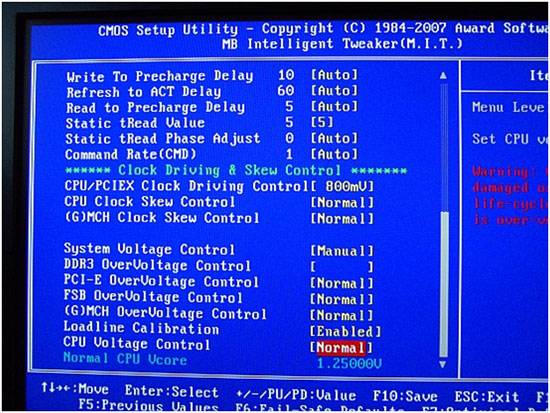
Write To Precharge Delay
Again, this setting is offset by -10. The range of interest in BIOS is between 6 and 13 (16 to 23 actual). Higher numbers mean less performance, but help with stability.
Refresh To Act Delay (aka tRFC)
48-72 is the range of interest, lower settings can have a huge impact on memory bandwidth at the expense fo stability. For benchmarking 48-55 is preferred. For stability testing at high memory speeds start high (72) and work downwards slowly.
Read to Precharge Delay (tRTP)
A setting of 4-6 is usually sufficient across the entire range of FSB and memory speeds that this board offers. 4 is tight and used for benchmarking, while a setting of 5-6 gives stability as FSB and memory speed is scaled. For high FSB speeds with quad-core processors or 4GB memory overclocking a setting of 6 may be preferable.
Static tREAD Value
This setting is more commonly known as Performance Level or tRD and is the most effective chipset performance register available for adjustment on this motherboard. As FSB and memory speed are scaled, tRD and Northbridge voltage will have to be increased to accommodate the additional data throughput. The idea when seeking outright system performance is to run the tightest tRD possible at any given FSB or memory speed. Our retail sample board maxed out at a tRD of 6 at 400 FSB using the 2:1 divider. For 65nm dual core processors, a tRD setting of 7 is usable up to 500FSB. For lower chipset voltages and stability increase tRD by +1 over these figures if stability issues are experienced.
tRD Phase Shift
The user selectable scale runs from 1-31. Setting Auto results in a selection of 0, which means both memory channels remain at the default Performance Level. tRD phase shift allows the user to run either memory channel at a lower Performance Level than the applied BIOS setting of Static tRD Delay. The scale used by Gigabyte is not really intuitive, as it does not immediately show the user which of the memory channel phases are being lowered - at any of the settings available. The number of available or effective phases varies according to the memory divider being used. The explanation of how the phases are configured is outside the scope of this review and deserves a write-up of its own. Look for an upcoming article on AnandTech that will fully describe Intel chipset overclocking in layman terms.
For now, we will stick with the basic rule that a tRD phase adjustment subtracts 1 from the static tRD level at a given point in the FSB/memory read transfer cycle. This function only needs to be used (experimented with) when using FSB speeds that fall between two Performance Level (tRD) FSB limits. Every increase in Performance Level requires a suitable rise in FSB speed to make up the associated memory access latency and bandwidth deficit. If a small hike past a Performance Level limit at a given FSB is made (for additional processor speed), valuable access latency and memory bandwidth is lost unless the rise in FSB speed is very substantial.
With the FSB limits of quad-core processors falling below 470FSB and requiring a tRD of 7-8 in most cases, it can be far easier both in terms of BIOS tuning and board voltages to retain a low tRD of 5 or 6 at around 400FSB using a higher CPU multiplier. The gray area in terms of performance falls between 420-450FSB, where a tRD of 6 starts requiring very high levels of Northbridge voltage to hold steady. When benchmarking with a motherboard there may be instances (due to chipset limitations) where running these intermediate FSBs is the only option. In this instance, it makes sense to apply tRD phase shifts in an attempt to minimize chipset latency loss.
We look at the memory bandwidth and access latency changes at all 31 steps of tRead Phase Adjust below. Please note, the table is for demonstration purposes only; actual board abilities and maximum operating conditions may differ according to a number of variables. We expect that users with quad-core processors will use the 1:2 memory divider at all times, to maximize memory bandwidth at the FSB levels that are available to them. Dual-core CPUs have access to higher stable FSB speeds, in which case using one of the lower dividers to peg memory speed to acceptable and operable speeds will be required.
 |
The rows highlighted in the darker blue represent the most aggressive Phase Adjust points. The table above shows that using the 1:2 memory divider, tRD Phase Adjust settings of 3, 7, 11, 15, 19, 23 (non boot), 27 (non boot), and 30 (non boot) are the most aggressive. In fact, these settings draw an almost complete parallel to running a tRD of 6. To increase FSB potential, some of the less aggressive phase shift settings will need to be used. Again, we stress that most users will not find much to gain in these adjustments. However, for those who are truly passionate about performance tweaking, tRD phase adjustments represent a method of almost linear memory bandwidth and latency scaling throughout the range of chipset capability with a particular CPU. These kinds of tweaks generally bear interest to those who benchmark for maximum scoring potential. Retaining chipset latency can be the difference between a record and tenth place, as there is little to separate overall processor speeds at the top of the Futuremark Orb these days.
We were intrigued by the fact that tRD Phase Shift settings of 23, 27, and 30 would not boot even if we changed Northbridge straps. We managed to get a peek at just how aggressive the non-booting registers were. The Northbridge was set to the 1333 chipset strap with the 1:2 memory divider ratio and 1N command rate at a tRD of 8. We then set a tRD phase shift setting to 23, 27 or 30 and proceeded to boot into Windows. Once Windows had booted up, we lowered the tRD back down to 7 via Memset. The interesting fact is that the board was fully capable of running the Prime95 Torture test at these points for significant periods of time. This points the finger at an inadequate BIOS, rather than a chipset limitation. What is also interesting is that the registers of 23 and 27 are actually more aggressive than running a flat tRD of 6. This implies that these registers may be cross-linked to other hidden chipset performance enhancing registers.


37 Comments
View All Comments
Frumious1 - Thursday, January 3, 2008 - link
What are you, the jilted lover of Raja or something? Seriously, I can't say I blame the AT crew for taking a break. Me and my family certainly did our fair share of slacking off over the holidays.Merry Christmas, Foxy Scrooge....
8steve8 - Wednesday, January 2, 2008 - link
i just got 8gb od ddr2 800 1.8v for $180 shipped from newegg.8GB of DDR3 costs $1,150 shipped from newegg...
thats not at typo.
DDR3 is irrelevant for now.
10x cost for 3% perf boost...
I'm not even going to read this review.
Kougar - Wednesday, January 2, 2008 - link
This makes no sense. Gigabyte offers GTL controls on the P31-DS3L, values are: 0.636, 0.603, 0.566, 0.54. Why offer them on a $80 budget board but not a ~$300 X48T end-of-the-world board?? I was expecting them to be there when I heard about the redesign.This was a great review, and I am still reading/rereading it to absorb the info. I had a few questions though... You said FSB Overvoltage control requires 1.4v for both processors, and stock is 1.15v?? I never touched this setting by more than +1 with my Q6600, but it might explain a few things. How or where did you find out what the stock VTT value was, as I wish to be able to look up this info myself for future reference and check the P35 version.
Rajinder Gill - Wednesday, January 2, 2008 - link
I used a DMM and probed both the supply mosfet and GTL transistors.Regards
Raja
Kougar - Wednesday, January 2, 2008 - link
Thanks for your reply! Are there any guides or what do you recommend for novice multimeter users trying to discern which mainboard components power what. I don't mind doing the research, I just need a pointer at where to get started. I have tried before but was not sure if I was measuring the correct components.Just for proof, here is a screenie of the P31 DS3L $75 board's GTLREF menu: http://i111.photobucket.com/albums/n129/Chanur64/I...">http://i111.photobucket.com/albums/n129/Chanur64/I...
I can't fathom why the X48-DQ6 lacks this, could they be waiting to add it in later when the BIOS is more mature?
PLaYaHaTeD - Wednesday, January 2, 2008 - link
Since nobody cares to ask, I will go ahead:When can we buy an X48 Motherboard, along with a Q9450 cpu? How can you give such a comprehensive preview, and talk about recommendations without addressing a release date?
If some of the rumors are true about X48/Wolfdale/Yorkfield being delayed to possibly march, then wouldn't it be irrelevant to speak about recommending this product 2-3 months before it will even be available?
Gary Key - Friday, January 4, 2008 - link
ETA of the X48 boards is unknown. They are ready, from a BIOS viewpoint the Gigabyte boards need some more work but the ASUS boards that will be reviewed next week are about 97% there. Boards have been manufactured by all of the majors, it is up to Intel to pull the trigger. It was going to be in December, moved to 1/7/08, moved to 1/21/08, and is now in a holding pattern waiting on X38 stocks to clear out to some degree, which is surprising as most of the suppliers will move X38 downward to replace the mid-market P35 boards.The Q9450 and others will be announced shortly and official launch dates will be available at that time. Once again, up to Intel, but after the Phenom launch, they have no real reason to hurry up. The reason for the previews is provide just that, a preview, but we were expecting (along with Gigabyte/ASUS/MSI) that boards would be launched by the 21st of this month.
minimeat - Wednesday, January 2, 2008 - link
Good review on the BIOS features, i've been looking for this kind of detail for each timing number to be explained for a while, as none of this information is in the Gigabyte manual for any of their motherboards (HINT HINT).Anyways, you forgot to explain one really important number that i have been wondering about for a while, the Refresh to ACT Delay. Can someone please explain this number, either update the review or post it here, it would be much appreciated. I noticed that they had it set to 60 in the review, and there is no Auto option inherent in the motherboard's bios for this number, and i have no clue what it does. Thanks!
Glenn - Wednesday, January 2, 2008 - link
Looks like Anands crew spent plenty of time with this board! Amazing that no comparison benchmarks are shown against more mainstream boards like 965s, P35s or some AMD flavors? All that work with very little usefullness outside of early adoptee's!Gary Key - Friday, January 4, 2008 - link
Hi,We will have a Intel chipset comparison roundup the week of the 28th, maybe earlier if Intel decides to launch this product according to the last timeline. We will have the ASUS X48 boards up next week with a very detailed MCH overview and the MSI X48 board the week after with some Quad CrossFire loving if the drivers make it. These previews are concentrating on getting the most out of the board, the roundup will concentrate on comparisons to other available products.