The Era of Tera: Intel Reveals more about 80-core CPU
by Anand Lal Shimpi on February 11, 2007 5:44 PM EST- Posted in
- CPUs
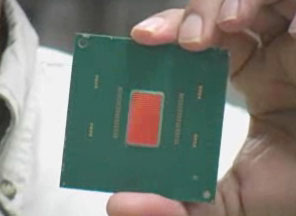
The Chip
As its name implied, the Teraflops Research Chip is a research vehicle and not a product. Intel has no intentions of ever selling the chip, but technology used within the CPU will definitely see the light of day in future Intel chip designs.
The Teraflops chip is built on Intel's 65nm process and features a modest, by today's standards, 100M transistors on a 275mm^2 die. As a reference point, Intel's Core 2 Duo, also built on a 65nm process, features 291M transistors on a 143mm^2 die. The reason the Teraflops chip is large given its relatively low transistor count is that there's very little memory on the chip itself, whereas around half of Intel's Core 2 is made up of L2 cache. Other than being predominantly logic circuits, the Teraflops chip also has a lot of I/O circuitry on it that can't be miniaturized as well as most other circuits resulting in a larger overall chip size. The chip features 8 metal layers with copper interconnects.
The Teraflops chip is built on a single die composed of 80 independent processor cores, or tiles as Intel is calling them. The tiles are arranged in a rectangle 8 tiles across and 10 tiles down; each tile has a surface area of 3mm^2.
The chip uses a LGA package like Intel's Core 2 and Pentium 4 processors, but features 1248 pins. Of the 1248 pins on the package, 343 of them are used for signaling while the rest are predominantly power and ground.
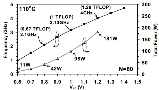
The chip can operate at a number of speeds depending on its operating voltage, but the minimum clock speed necessary to maintain its teraflop name is 3.13GHz at 1V. At that speed and voltage, the peak performance of the chip with all 80 cores active is 1 teraflop while drawing 98W of power. At 4GHz, the chip can deliver a peak performance of 1.28 TFLOP, pulling 181W at 1.2V. On the low end of the spectrum, the chip can run at 1GHz, consuming 11W and executing a maximum of 310 billion floating point operations per second.


25 Comments
View All Comments
creathir - Monday, February 12, 2007 - link
With all of this wonderful multi-core bliss, is the software side of things. Multicore means the software needs to be written asymentrically. This will be an incredibly hard challenge, especially on real time applications such as video games. The concept is fantastic, but the proof is in the pudding as they say. I do find Intel's routing technology to be quite interesting, especially the idea of stacking the L1/L2 memory on top (or below rather;)) the cores. The interconnect on them, how would this work exactly I wonder? Should be interesting to see what all 3 of these companies come out with in the coming years. I suppose the nay sayers of Moore's law will be once again disproven...- Creathir
Goty - Sunday, February 11, 2007 - link
So basically it's a Cell processor on steroids. Other than the chip stacking, what's so new about it? People have been talking about 3D packaging for a year or two now, and not just Intel.SocrPlyr - Monday, February 12, 2007 - link
In a way, yes. And in a lot of ways, no. Yes the individual tiles are floating point units, but this chip is not meant to be a functional replacement for anything like the cell is trying to be. You really cannot compare this chip to anything available on the market. It is only a proof of concept. The choice of tiles that are floating point units was probably due to the fact that ultra high performance needs generally are nearly completely FP dependent. When testing and playing with this thing those types of applications are easy to come by. To be honest this chip seems a lot like a DSP chip, and mentioning those you will realize that the Cell processor is anything but an altered one of those. Really on all sides there has been little technology that is completely new, just better implementations.oldhoss - Sunday, February 11, 2007 - link
I'll bet that SOB would give two 8800GTX's a run for their money....CPU-limited be damned! ;-Dmino - Sunday, February 11, 2007 - link
"Since the per-die area doesn't increase, the number of defects don't go up per die."Any sensible person knows that defect-rate is(mostly) dependent on the number of functional units(i.e. transistors), provided the defect-rate off a single unit is set.
The fact that it is NOW mostly tied to die-area is caused exactly by the fact we do NOT use stacked-die aproach yet.
Otherwise a nice news piece. Thanks AT.
mino - Sunday, February 11, 2007 - link
sorry for typpos...notposting - Sunday, February 11, 2007 - link
The picture above this shows the Terascale slide:
http://images.anandtech.com/reviews/cpu/intel/tera...">http://images.anandtech.com/reviews/cpu/intel/tera...
sprockkets - Sunday, February 11, 2007 - link
We have a solution to the problem of ever increasing CPU speed. My question is, who here needs it?For those who need to open 80 Firefox tabs, video encoding, virus scanning and watching a HD movie, at the same time?
Data sets did need to get bigger, but check this out: Music files started out at small sampling rates till about Win98 they got to the cd standard. It stopped there since no one needs it bigger than that, that is, 44.1khz and 16 bit resolution. If you can hear 96/192khz 24bit music better, fine, but we have others saying that 128kbps mp3 was cd quality.
Video resolutions made their way from 640x480 to now around 1600x1200, and widescreen varients of that. Color depth sits at around 32bit. Can you see it improving beyond that?
OK, so we can what, go 3D now, holographic?
Sorry to you Intel and AMD, but the vast majority of the people you sell your technology to can live off a $30 processor and $50 of RAM, the smallest HDD, and a $30 optical drive which does everything.
Would be cool to see a motherboard with built in DDR3 or 4 memory for the cpu/gpu AMD Fusion core, and have 2GB of it, with 32GB of flash built on as well. Let's go for silent computing, you know, back in the day when all processors only had tiny heatsinks on them!!!
joex444 - Monday, February 12, 2007 - link
What part of the article was confusing to you?NOT FOR RETAIL SALE, COMMERCIAL USES ONLY.
I got the idea, guess you didn't. PWNT!
Larso - Monday, February 12, 2007 - link
So, why did we ever bother invent plastic materials? Or why invent the laser? The laser is a good example of an invention that was expected to be a useless curiosity but turned out to be hugely usefull.But this case isn't even comparable to that. There are indeed problems waiting to be solved with this solution. All servers with more than a handfull of CPU's could be cut down in size and power usage tremendously, and what about supercomputers? They are going to be extra extremely powerfull when they change to this kind of cpu's.
And by the way, you have to be quite narrowminded to not see the (sales) potential of supercomputing at home. Lets have computer games with scary intelligent AI's :)