Intel Demonstrates new 45nm Transistors and Conroe's Successor
by Anand Lal Shimpi on January 27, 2007 12:00 AM EST- Posted in
- CPUs
More Efficient Transistors
The basic function of a transistor as found in modern day microprocessors is to act as a switch with two states: on and off. When the transistor is on, current is allowed to flow from one terminal to the other (source to drain), and when it is off current shouldn't flow. Making enough current flow when it should and minimizing the amount that flows when it shouldn't is one of the major hurdles to making smaller transistors that run cooler/faster.
Below we have a typical CMOS transistor diagramed and labeled:
![]()
The voltage present at the Gate and the Source will determine whether or not current will flow in the transistor. Intel's 45nm process makes significant changes to two of the components in this transistor diagram: the gate electrode and the gate dielectric.
You can probably guess that as transistors get smaller, all of the parts of the transistor get smaller as well. The problem is that when some of these features get too small, they start behaving inappropriately. Case in point is the gate dielectric; with Intel's 90nm and 65nm processes, the gate dielectric was shrunk to a thickness of 1.2nm - the equivalent of about 5 atoms. The benefit of a very thin gate dielectric is that it increases the gate field effect, which increases drive current and reduces Source-drain leakage current. However, with such a thin gate dielectric electrons can tunnel directly through the layer and show up as leakage current - in other words, current would flow when it was not supposed to, translating into power wasted. On an individual transistor scale it's not such a big deal, but when you keep in mind that Penryn will have around 410 million of these transistors (820 million for quad-core) the leakage current/power draw does add up.
At 1.2nm, the gate oxide/gate dielectric in Intel's 90nm and 65nm transistors was as thin as Intel could make it without losing a great deal of power due to gate oxide leakage current. In order to make the move to 45nm Intel had to do something to thin the gate oxide without drastically increasing gate oxide leakage current.
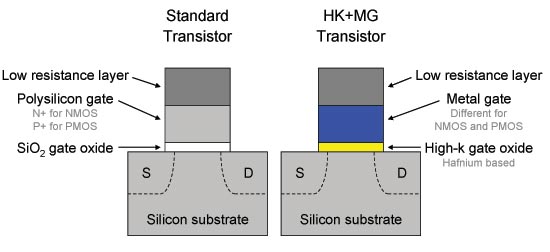
Intel solved the gate oxide leakage problem by replacing the SiO2 gate dielectric with a material that has a higher k-value, in this case a Hafnium based material. A high-k dielectric here actually increases drive current at the same thickness as the previous SiO2 dielectric, while reducing gate leakage as well. Intel isn't disclosing how thick the Hafnium gate dielectric layer is in its 45nm transistors, but we do know that it is thicker than the 1.2nm SiO2 gate dielectric used in previous 90nm and 65nm transistors.
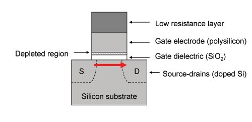
The second problem Intel is addressing with its 45nm transistors is a fundamental issue with the polysilicon gate electrode. The role of the gate electrode is important as it is what enables current to be driven through the transistor and as such it plays a role in how much current can be delivered. The polysilicon material that the gate electrode is made of has a tendency to form a region of depleted conducting carriers at the bottom of the gate, which reduces the drive strength of the transistor (less current flows when it needs to).
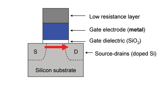
Intel's new 45nm transistors solve this problem by replacing the polysilicon gate electrode with a metal gate electrode, which completely eliminates the depleted region thus increasing the drive current.
Intel has been researching this High-k + Metal Gate (HK+MG) combination in transistors for a handful of years now, with hundreds of material options for metal gate electrodes and high-k dielectrics. The actual combination of high-k and metal gate material isn't being disclosed at this time, most likely to protect Intel's research and maintain the manufacturing advantage as long as possible. Intel expects that no other company will have HK+MG transistors until they reach 32nm or later.
The tangible advantages of these changes in materials in combination with the smaller 45nm process are quite large. According to Intel, the move from 65nm to 45nm yields a 30% reduction in transistor switching power because of the simple fact that smaller transistors have less parasitic capacitance and require less power to switch on and off.
Because of the combination of a high-k dielectric and the metal gate electrode, Intel is quoting a greater than 20% improvement in switching speed compared to its 65nm transistors. At the same speed as its 65nm transistors, there's a greater than 5x reduction in source-drain leakage power and a greater than 10x reduction in gate oxide leakage power; the latter is due entirely to the use of a high-k dielectric in the transistor. The end results of all of this are more power efficient processors, the first of which we should see by the end of this year.


59 Comments
View All Comments
tygrus - Sunday, January 28, 2007 - link
100mm^2 is twice the area as 50mm^2.100mm^2 means the mm is squared not the 100.
10mm x 10mm = 100mm^2
5mm x 10mm = 50mm^2
lopri - Saturday, January 27, 2007 - link
I am more interested in the long-awaited introduction of integrated memory controller from Intel CPU. IIRC, it's supposed to happen with 45nm process, which makes me curious whether Nehalem will be the one. This will likely happen in parallel with HSI, or High Speed Interconnect, which is supposed to be compatible with PCI-Express 2. (How that can be done - beats me) Nehalem might as well be 'simply' Core 2 Duo + IMC as Hammer was Athlon XP + IMC.While this is obviously Intel's PR piece, it is an undeniable truth that AMD doesn't even have anything for such. It's foolish to think that AMD wouldn't be bragging had they have made an advance like this.
A good news for AMD is that the processing power for desktop has, to my eyes, reached to the point that it's sufficient for majority of daily computing for forseable future. In other words, majority of people will not likely take advantage of any more computing power (be it speed or multitasking) than what current CPUs can process. I wonder AMD will turn to a totally different direction from this hopeless speed race.
IntelUser2000 - Sunday, January 28, 2007 - link
HSI?? High Speed Interconnect?? That's a new one. No, its CSI, and it stands for Common System Interface, which was originally named because it was supposed to bring socket compatibility between Itanium and Xeon, or at least the electrical part of it.
lopri - Sunday, January 28, 2007 - link
Got me there. Yah it's CSI. Thanks for the correction.MadBoris - Saturday, January 27, 2007 - link
Maybe I am missing something here, but where is the chipset information.Is this going to be on a new chipset, or 775 compatible?
Knowing Intel, it's a new chipset, they love to stimulate the economy (their economy) with new chipsets all the time.
Any word?
Groovester - Saturday, January 27, 2007 - link
Due to HK+MG's 20% higher switching rate and much lower leakage currents, shouldn't we expect ("more power efficient processors") both higher clock speeds AND lower TDP, even with a slightly higher transistor count?IntelUser2000 - Sunday, January 28, 2007 - link
No. First thing is the recent roadmaps shown by HKEPC say it doesn't lower power, part of the reason is to increase yields, the other has to be clock speeds.
(If you want to read further, go ahead, but it tends to be long)
It does present much lower leakage, but there is a caveat: "Intel is quoting a greater than 20% improvement in switching speed compared to its 65nm transistors. At the same speed as its 65nm transistors, there's a greater than 5x reduction in source-drain leakage power and a greater than 10x reduction in gate oxide leakage power"
The source-drain is the reason for leakage power when the transistor is active(meaning its on), and gate oxide leakage power is for idle. Read the second sentence carefully: "At the same speed as its 65nm transistors...
It means if Intel wants to take advantage of the 20% increase in clock speed, they'll likely have to forgo the reduction in active leakage power. Contrary to what most news sites wants you to believe, leakage isn't of a big problem as they want you to believe(most of the reason is that they want hits to the webpage), especially on a power optimized CPU like Conroe. The exponential leakage increase every shrinking process would have been true if the companies like Intel did nothing about it. Of course they can't allow that to happen and added their own optimizations and enhancements. Its not a complete elimination either, but a 5x reduction.
If they want to keep the 65W, we'll have to base it on the E6700, which is at 2.66GHz. With 1333MHz FSB, I can see mainstream dual core devices clock at 3.66/3.83GHz. Since it seems Intel is using a "family TDP", the 65W figure would likely have to be made to fir the 3.66/3.83GHz part. They may be able to tweak it higher and go 4.0GHz or lower power, but that tweaks will probably be seen on the Nehalem derivatives.
2.66GHz x (20% faster) = 3.2GHz
30% lower power = 0.7 But
0.7 x 1.44(going beyond 3.2GHz will require greater than nominal voltages, which means more power. But faster clock speeds also mean more power. 20% higher voltage x 20% higher clock = 44% higher power)~1.00
Sure some of you guys like to lower voltages below nominal and don't overclock, but possible sacrifice in stability won't be seen as good for the corporate market and Intel generally.
So approximately same power consumption
Now if you kept up to the roadmaps you might say, what about the 1333MHz 3.0GHz parts that's also said to be at 65W?? First, look at the X6800 with 75W TDP. Well, since the 3.0GHz/1333MHz FSB parts come a year later after Conroe, Intel will have time to tweak it.
IntelUser2000 - Saturday, January 27, 2007 - link
If we derive clock speed numbers from Anandtech's Spring IDF 2005 article about Presler, we should be able to come up with a similar number :).http://www.anandtech.com/showdoc.aspx?i=2362">http://www.anandtech.com/showdoc.aspx?i=2362
"It looks like the chip was running at 2.0GHz, which isn't too impressive in itself, until you remember that we're talking about a 65nm processor here whose launch is over a year away."
45nm Quad core Desktop parts running at 1.86GHz
45nm Dual core desktop parts running at 2.13GHz
Now Presler came with 3.6GHz for the mainstream(Pentium D 960) and 3.73GHz with the enthusiast(Pentium Extreme Edition 3.73GHz). If we apply similar increase between prototype and final product, we get:
45nm Quad core desktop: 3.46GHz @ 1066MHz FSB/3.5GHz @ 1333MHz FSB(45nm parts support half step dividers)
45nm Dual core desktop: 4.0GHz @ 1333MHz FSB
Since the TDP is not supposed to go down, we can expect all the power headroom to be translated to clock speed. The estimations also match the roadmaps.
Staples - Saturday, January 27, 2007 - link
A price drop. It is ridiculous that C2Ds have not dropped a cent since they came out 6+ months ago.MarkM - Saturday, January 27, 2007 - link
http://www.nytimes.com/2007/01/27/technology/27chi...">http://www.nytimes.com/2007/01/27/techn...63262&am...