Intel Demonstrates new 45nm Transistors and Conroe's Successor
by Anand Lal Shimpi on January 27, 2007 12:00 AM EST- Posted in
- CPUs
They often say that the bigger a company gets, the more difficult it is to make sweeping changes to fix problems. Analogous to quickly turning a small boat vs. a large tanker, no one would have ever expected Intel to change so quickly over the past several months.
It's not only on the performance side that we've seen tremendous change; after all, it just took a new architecture to do that. No, the change we're speaking of here is in how Intel conducts itself, how freely it shares information today and how very different the road to 45nm has been compared to the move to 90nm or 65nm.
Today Intel is announcing a number of details on its 45nm process node, including official details on the first family of 45nm processors due out later this year. The announcements themselves, as you will soon see, are impressive enough, but arguably more interesting is the amount of detail Intel is giving away at this point. In the past we've had to go to sources other than official Intel channels for this sort of information, but that has all changed with the new Intel.
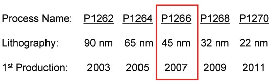
On track for first production by the end of 2007 with the Penryn family of processors (mobile, desktop and server), is Intel's 45nm manufacturing process. As with any move to smaller transistors, the 45nm node will make chips smaller and run faster. Intel is actually seeing good feature scaling with its 45nm process, quoting a ~2x improvement in transistor density. In other words, if you took a 100mm^2 65nm chip and built it on Intel's 45nm process, it would be roughly a 50mm^2 chip after the shrink. While logic and cache structures generally end up scaling very well with a process shrink, I/O structures (e.g. main memory interface circuits) don't which is why the improvement in transistor density is roughly and not exactly 2x.
Of course, in the past Intel has usually coupled new process technology with more features so you shouldn't expect to see 45nm Penryn chips as simply smaller Core 2 Duos. We will look at Penryn's die in a moment, but a larger cache, SSE4 and other unannounced microarchitectural enhancements can be expected.
The story of Intel's 45nm process doesn't end with details on its feature scaling however. Intel has made some fairly significant changes to the transistors themselves that make them more efficient than normal.


59 Comments
View All Comments
tygrus - Sunday, January 28, 2007 - link
100mm^2 is twice the area as 50mm^2.100mm^2 means the mm is squared not the 100.
10mm x 10mm = 100mm^2
5mm x 10mm = 50mm^2
lopri - Saturday, January 27, 2007 - link
I am more interested in the long-awaited introduction of integrated memory controller from Intel CPU. IIRC, it's supposed to happen with 45nm process, which makes me curious whether Nehalem will be the one. This will likely happen in parallel with HSI, or High Speed Interconnect, which is supposed to be compatible with PCI-Express 2. (How that can be done - beats me) Nehalem might as well be 'simply' Core 2 Duo + IMC as Hammer was Athlon XP + IMC.While this is obviously Intel's PR piece, it is an undeniable truth that AMD doesn't even have anything for such. It's foolish to think that AMD wouldn't be bragging had they have made an advance like this.
A good news for AMD is that the processing power for desktop has, to my eyes, reached to the point that it's sufficient for majority of daily computing for forseable future. In other words, majority of people will not likely take advantage of any more computing power (be it speed or multitasking) than what current CPUs can process. I wonder AMD will turn to a totally different direction from this hopeless speed race.
IntelUser2000 - Sunday, January 28, 2007 - link
HSI?? High Speed Interconnect?? That's a new one. No, its CSI, and it stands for Common System Interface, which was originally named because it was supposed to bring socket compatibility between Itanium and Xeon, or at least the electrical part of it.
lopri - Sunday, January 28, 2007 - link
Got me there. Yah it's CSI. Thanks for the correction.MadBoris - Saturday, January 27, 2007 - link
Maybe I am missing something here, but where is the chipset information.Is this going to be on a new chipset, or 775 compatible?
Knowing Intel, it's a new chipset, they love to stimulate the economy (their economy) with new chipsets all the time.
Any word?
Groovester - Saturday, January 27, 2007 - link
Due to HK+MG's 20% higher switching rate and much lower leakage currents, shouldn't we expect ("more power efficient processors") both higher clock speeds AND lower TDP, even with a slightly higher transistor count?IntelUser2000 - Sunday, January 28, 2007 - link
No. First thing is the recent roadmaps shown by HKEPC say it doesn't lower power, part of the reason is to increase yields, the other has to be clock speeds.
(If you want to read further, go ahead, but it tends to be long)
It does present much lower leakage, but there is a caveat: "Intel is quoting a greater than 20% improvement in switching speed compared to its 65nm transistors. At the same speed as its 65nm transistors, there's a greater than 5x reduction in source-drain leakage power and a greater than 10x reduction in gate oxide leakage power"
The source-drain is the reason for leakage power when the transistor is active(meaning its on), and gate oxide leakage power is for idle. Read the second sentence carefully: "At the same speed as its 65nm transistors...
It means if Intel wants to take advantage of the 20% increase in clock speed, they'll likely have to forgo the reduction in active leakage power. Contrary to what most news sites wants you to believe, leakage isn't of a big problem as they want you to believe(most of the reason is that they want hits to the webpage), especially on a power optimized CPU like Conroe. The exponential leakage increase every shrinking process would have been true if the companies like Intel did nothing about it. Of course they can't allow that to happen and added their own optimizations and enhancements. Its not a complete elimination either, but a 5x reduction.
If they want to keep the 65W, we'll have to base it on the E6700, which is at 2.66GHz. With 1333MHz FSB, I can see mainstream dual core devices clock at 3.66/3.83GHz. Since it seems Intel is using a "family TDP", the 65W figure would likely have to be made to fir the 3.66/3.83GHz part. They may be able to tweak it higher and go 4.0GHz or lower power, but that tweaks will probably be seen on the Nehalem derivatives.
2.66GHz x (20% faster) = 3.2GHz
30% lower power = 0.7 But
0.7 x 1.44(going beyond 3.2GHz will require greater than nominal voltages, which means more power. But faster clock speeds also mean more power. 20% higher voltage x 20% higher clock = 44% higher power)~1.00
Sure some of you guys like to lower voltages below nominal and don't overclock, but possible sacrifice in stability won't be seen as good for the corporate market and Intel generally.
So approximately same power consumption
Now if you kept up to the roadmaps you might say, what about the 1333MHz 3.0GHz parts that's also said to be at 65W?? First, look at the X6800 with 75W TDP. Well, since the 3.0GHz/1333MHz FSB parts come a year later after Conroe, Intel will have time to tweak it.
IntelUser2000 - Saturday, January 27, 2007 - link
If we derive clock speed numbers from Anandtech's Spring IDF 2005 article about Presler, we should be able to come up with a similar number :).http://www.anandtech.com/showdoc.aspx?i=2362">http://www.anandtech.com/showdoc.aspx?i=2362
"It looks like the chip was running at 2.0GHz, which isn't too impressive in itself, until you remember that we're talking about a 65nm processor here whose launch is over a year away."
45nm Quad core Desktop parts running at 1.86GHz
45nm Dual core desktop parts running at 2.13GHz
Now Presler came with 3.6GHz for the mainstream(Pentium D 960) and 3.73GHz with the enthusiast(Pentium Extreme Edition 3.73GHz). If we apply similar increase between prototype and final product, we get:
45nm Quad core desktop: 3.46GHz @ 1066MHz FSB/3.5GHz @ 1333MHz FSB(45nm parts support half step dividers)
45nm Dual core desktop: 4.0GHz @ 1333MHz FSB
Since the TDP is not supposed to go down, we can expect all the power headroom to be translated to clock speed. The estimations also match the roadmaps.
Staples - Saturday, January 27, 2007 - link
A price drop. It is ridiculous that C2Ds have not dropped a cent since they came out 6+ months ago.MarkM - Saturday, January 27, 2007 - link
http://www.nytimes.com/2007/01/27/technology/27chi...">http://www.nytimes.com/2007/01/27/techn...63262&am...