AMD's 65nm Preview Part 2 - The Plot Thickens (Updated with Information from AMD)
by Anand Lal Shimpi on December 21, 2006 12:12 AM EST- Posted in
- CPUs
Of Die Sizes, Voltages and Power
When we published our first Brisbane article, an astute reader pointed out that AMD appeared to have rather poor die scaling with the 90nm to 65nm transition. Given perfect scaling, you'd expect a 65nm shrink of a 90nm core to be approximately 52% the size of the larger core. Looking at Brisbane, AMD went from 183 mm^2 with its 90nm Windsor core down to 126 mm^2 at 65nm, making the newer core almost 69% the size of the older one. If we look at Intel, most of its die shrinks are coupled with new architectural functionality or larger caches, so it's not unusual to see scaling in the 70 - 80% range. However, with Brisbane, transistor counts remained the same according to AMD (approximately 154M) yet we still saw relatively poor scaling with die size. The table below provides some reference points for die sizes and transistor counts:
| CPU | Manufacturing Process | Die Size | Transistor Count |
| AMD Windsor | 90nm | 183 mm^2 | 154M |
| AMD Brisbane | 65nm | 126 mm^2 | 154M |
| Intel Smithfield | 90nm | 206 mm^2 | 230M |
| Intel Presler | 65nm | 162 mm^2 | 376M |
| Intel Prescott-2M | 90nm | 135 mm^2 | 169M |
| Intel Cedar Mill | 65nm | 81 mm^2 | 188M |
Note that when Intel moved from 90nm to 65nm with its Smithfield to Presler transition, the 65nm core ended up being almost 79% the size of the older core. However when you take into account that transistor count went from 230M to 376M, all of the sudden the scaling looks a lot better. The bulk of that increase in transistor count was Presler's extra L2 cache, which happens to shrink quite well, so it's unfortunately not the best comparison. Looking at Prescott-2M to Cedar Mill, Intel saw very good scaling with a 40% smaller chip at 65nm (60% the size of the 90nm core).
Obviously some structures within a core will shrink better than others in terms of surface area, so perfect scaling isn't necessarily a target reality, but one of the questions we asked AMD was why the new core is seemingly so big. We couldn't get an official answer from AMD as many of the folks that would be able to get us such a thing were on vacation and unreachable, but the gist is that coupled with the fact that not everything scales well with manufacturing process, this is AMD's first 65nm chip, and AMD tends to make many improvements to its manufacturing process over time. The chip we're comparing Brisbane to was made at the pinnacle of AMD's 90nm manufacturing cycle, so it's quite possible that, with time, AMD will improve its 65nm process to the point where a smaller Brisbane would be possible. Until we can get a more technical explanation from AMD, that's the best we can report on this issue. On to number two...
We weren't impressed with the power consumption of Brisbane at all in our first review; while it was lower than its 90nm counterpart, in many cases it wasn't all that much lower. Once again this is an issue of comparing a very mature 90nm process with AMD's first 65nm chips. You see, the voltages that Brisbane will be manufactured at range from 1.250V to 1.350V, with the coolest running, highest overclocking, least power consuming chips running at 1.250V and the worst examples running at 1.350V. Both of our Brisbane samples, the 5000+ and 4800+, ran at 1.350V. Note that our 90nm 5000+ ran at 1.300V, a lower voltage than the newer 65nm core. The fact that many 65nm parts aren't at much lower voltages yet is why the highest clocked Athlon 64 X2s are still 90nm CPUs, such as the 5600+ which runs at 2.8GHz.
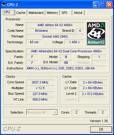
At some point in the future, AMD will hopefully be able to tune its manufacturing so that we will get lower voltage, lower wattage 65nm parts. This is also part of the reason why we encountered such dismal overclocking results with our 5000+. The 4800+ we tested fared no better, with our best overclock on stock cooling ending up at 2.837GHz (227 x 12.5) - not terrible for stock cooling, but not great either.
The impact of higher voltages on power consumption also applies to Intel as well. As you will see in our power comparison, in a number of cases our Core 2 Duo E6300 required even more power than the E6600 we tested last time. The reason being that our E6300 sample runs at a core voltage of 1.325V vs. 1.2625V for our E6600 sample. Just things to keep in mind as you look at the power results over the next few pages.
| CPU | Core Voltage of our Test Chip |
| AMD Athlon 64 X2 5000+ (90nm) | 1.3000V |
| AMD Athlon 64 X2 4600+ EE (90nm) | 1.2500V |
| AMD Athlon 64 X2 3800+ EE SFF (90nm) | 1.0750V |
| AMD Athlon 64 X2 5000+ EE (65nm) | 1.3500V |
| AMD Athlon 64 X2 4800+ EE (65nm) | 1.3500V |
| Intel Core 2 Duo E6600 (65nm) | 1.2625V |
| Intel Core 2 Duo E6400 (65nm) | 1.3125V |
| Intel Core 2 Duo E6300 (65nm) | 1.3250V |


52 Comments
View All Comments
theteamaqua - Thursday, December 21, 2006 - link
man i hope this thing overclocks like conroe.... otherwise no one will get quad fatherbut i already have E6400 @ 3.4GHz ...
might get Q6600 , Q6400 or Yorksfield or Altair ... ill what see what happens
clairvoyant129 - Thursday, December 21, 2006 - link
Right here,http://www.anandtech.com/cpuchipsets/showdoc.aspx?...">http://www.anandtech.com/cpuchipsets/showdoc.aspx?...
Nothing special though.
Better to stick with the 90nm X2 then this piece of junk.