NVIDIA's GeForce 8800 (G80): GPUs Re-architected for DirectX 10
by Anand Lal Shimpi & Derek Wilson on November 8, 2006 6:01 PM EST- Posted in
- GPUs
G80: A Mile High Overview
Now that we know a little more about the requirements and direction of DX10, we can take a deeper look at where NVIDIA has decided to go with the architecture of G80. We will be seeing a completely new design based around a unified shader architecture. While DX10 doesn't require a unified architecture, it certainly does make a lot of sense to move in that direction.
Inside G80, vertex, geometry, pixel shaders and more (more on this later) are all able to run on the same set of execution resources. In order to make this happen, the shader core needed to be made more general purpose and suitable for multiple usage scenarios. This is much like what we are used to seeing on a CPU, and as time moves on we expect these similarities to increase from both the CPU and GPU side. The design NVIDIA has come up, while very complex and powerful, is quite elegant. Here's a look at the block diagram for G80:
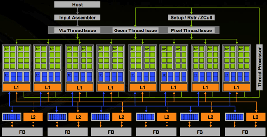
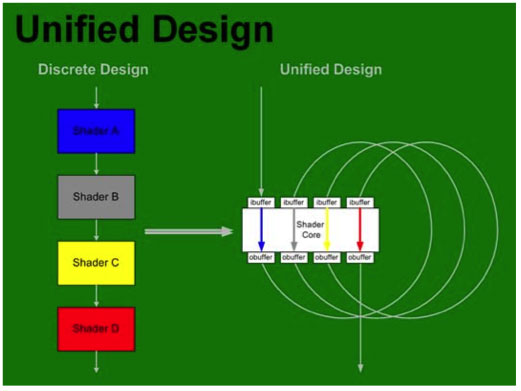
The architecture is able to use thread management hardware to dispatch different types of instructions on to the shader core. As vertices complete, their output can be used as input to geometry shaders back at the "top" of the shader core. Geometry shader output is then used as input to pixel shaders. Here's a quick conceptual representation of what we are talking about:
The sheer size of G80 is absolutely amazing; while NVIDIA wouldn't disclose exact die sizes let's look at the facts. The G80 chip is made up of 681 million transistors, more than a single core Itanium 2 or the recently launched Kentsfield, but manufactured on an almost old 90nm process. As a reference point, ATI's Radeon X1900 XTX based on the R580 GPU was built on a 90nm process yet it featured only 384 million transistors. NVIDIA's previous high-end GPU, the G71 based GeForce 7900 GTX was also built on a 90nm process but used only 278 million transistors. Any way you slice it, this is one huge chip. Architecting such a massive GPU has taken NVIDIA a great deal of time and money, four years and $475M to be exact. The previous record for time was almost 3 years at a lesser amount, but NVIDIA wouldn't tell us which GPU that was.
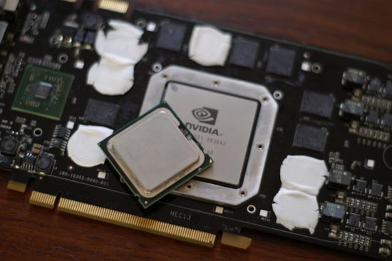
Intel's Quad Core Kentsfield on top, G80 on bottom
Despite very high clock speeds on the die and a ridiculous 681 million transistor count, power consumption of NVIDIA's G80 is quite reasonable given its target; on average, a G80 system uses about 8% more power than one outfitted with ATI's Radeon X1950 XTX.
You really start to get a sense of how much of a departure G80 is from previous architectures when you look at the shader core. Composed of 128 simple processors, called Stream Processors (SPs), the G80 shader core runs at a very high 1.35GHz on the highest end G80 SKU. We'll get into exactly what these stream processors are on the coming pages, but NVIDIA basically put together a wide array of very fast, specialized, but simple processors. In a sense, G80's shader core looks much like Cell's array of SPEs, but the SPs here are not nearly as independent as the SPEs in Cell.
Running at up to 1.35GHz, NVIDIA had to borrow a few pages from the books of Intel in order to get this done. The SPs are fairly deeply pipelined and as you'll soon see, are only able to operate on scalar values, thus through simplifying the processors and lengthening their pipelines NVIDIA was able to hit the G80's aggressive clock targets. There was one other CPU-like trick employed to make sure that G80 could have such a shader core, and that is the use of custom logic and layout.
The reason new CPU architectures take years to design while new GPU architectures can be cranked out in a matter of 12 months is because of how they're designed. GPUs are generally designed using a hardware description language (HDL), which is sort of a high level programming language that is used to translate code into a transistor layout that you can use to build your chip. At the other end of the spectrum are CPU designs which are largely done by hand, where design is handled at the transistor level rather than at a higher level like a HDL would.
Elements of GPUs have been designed at the transistor level in the past; things like memory interfaces, analog circuits, memories, register files and TMDS drivers were done by hand using custom transistor level design. But shaders and the rest of the pipeline was designed by writing high level HDL code and relying on automated layout.
You can probably guess where we're headed with this; the major difference between G80 and NVIDIA's previous GPUs is that NVIDIA designed the shader core at the transistor level. If you've heard the rumors of NVIDIA building more than just GPUs in the future, this is the first step, although NVIDIA was quick to point out that G80 won't be the norm. NVIDIA will continue to design using HDLs where it makes sense, and in critical areas where additional performance or power sensitive circuitry is needed, we'll see transistor level layout work done by NVIDIA's engineering. It's simply not feasible for NVIDIA's current engineering staff and product cycles to work with a GPU designed completely at the transistor level. That's not to say it won't happen in the future, and if NVIDIA does eventually get into the system on a chip business with its own general purpose CPU core, it will have to happen; but it's not happening anytime soon.
The additional custom logic and layout present in G80 helped extend the design cycle to a full four years and brought costs for the chip up to $475M. Prior to G80 the previous longest design cycle was approximately 2.5 - 3 years. Although G80 did take four years to design, much of that was due to the fact that G80 was a radical re-architecting of the graphics pipeline and that future GPUs derived from G80 will have an obviously shorter design cycle.


111 Comments
View All Comments
JarredWalton - Wednesday, November 8, 2006 - link
Page 17:"The dual SLI connectors are for future applications, such as daisy chaining three G80 based GPUs, much like ATI's latest CrossFire offerings."
Using a third GPU for physics processing is another possibility, once NVIDIA begins accelerating physics on their GPUs (something that has apparently been in the works for a year or so now).
Missing Ghost - Wednesday, November 8, 2006 - link
So it seems like by substracting the highest 8800gtx sli power usage result with the one for the 8800gtx single card we can conclude that the card can use as much as 205W. Does anybody knows if this number could increase when the card is used in DX10 mode?JarredWalton - Wednesday, November 8, 2006 - link
Without DX10 games and an OS, we can't test it yet. Sorry.JarredWalton - Wednesday, November 8, 2006 - link
Incidentally, I would expect the added power draw in SLI comes from more than just the GPU. The CPU, RAM, and other components are likely pushed to a higher demand with SLI/CF than when running a single card. Look at FEAR as an example, and here's the power differences for the various cards. (Oblivion doesn't have X1950 CF numbers, unfortunately.)X1950 XTX: 91.3W
7900 GTX: 102.7W
7950 GX2: 121.0W
8800 GTX: 164.8W
Notice how in this case, X1950 XTX appears to use less power than the other cards, but that's clearly not the case in single GPU configurations, as it requires more than everything besides the 8800 GTX. Here's the Prey results as well:
X1950 XTX: 111.4W
7900 GTX: 115.6W
7950 GX2: 70.9W
8800 GTX: 192.4W
So there, GX2 looks like it is more power efficient, mostly because QSLI isn't doing any good. Anyway, simple subtraction relative to dual GPUs isn't enough to determine the actual power draw of any card. That's why we presented the power data without a lot of commentary - we need to do further research before we come to any final conclusions.
IntelUser2000 - Wednesday, November 8, 2006 - link
It looks like putting SLI uses +170W more power. You can see how significant video card is in terms of power consumption. It blows the Pentium D away by couple of times.JoKeRr - Wednesday, November 8, 2006 - link
well, keep in mind the inefficiency of PSU, generally around 80%, so as overall power draw increases, the marginal loss of power increases a lot as well. If u actually multiply by 0.8, it gives about 136W. I suppose the power draw is from the wall.DerekWilson - Thursday, November 9, 2006 - link
max TDP of G80 is at most 185W -- NVIDIA revised this to something in the 170W range, but we know it won't get over 185 in any case.But games generally don't enable a card to draw max power ... 3dmark on the other hand ...
photoguy99 - Wednesday, November 8, 2006 - link
Isn't 1920x1440 a resolution that almost no one uses in real life?Wouldn't 1920x1200 apply many more people?
It seems almost all 23", 24", and many high end laptops have 1900x1200.
Yes we could interpolate benchmarks, but why when no one uses 1440 vertical?
Frallan - Saturday, November 11, 2006 - link
Well i have one more suggestion for a resolution. Full HD is 1920*1080 - that is sure to be found in a lot of homes in the future (after X-mas any1 ;0) ) on large LCDs - I believe it would be a good idea to throw that in there as well. Especially right now since loads of people will have to decide how to spend their money. The 37" Full HD is a given but on what system will I be gaming PS-3/X-Box/PC... Pls advice.JarredWalton - Wednesday, November 8, 2006 - link
This should be the last time we use that resolution. We're moving to LCD resolutions, but Derek still did a lot of testing (all the lower resolutions) on his trusty old CRT. LOL