NVIDIA's GeForce 8800 (G80): GPUs Re-architected for DirectX 10
by Anand Lal Shimpi & Derek Wilson on November 8, 2006 6:01 PM EST- Posted in
- GPUs
The 680i Platform
Alongside the GeForce 8800 GTX and GTS, NVIDIA is launching a brand new chipset for Intel processors, the nForce 680i (and 650i SLI and Ultra). Our own Wesley Fink has published an in-depth look at the new chipset, but we felt the release significant enough to comment on some of its features here in this review.
For the most part, competing with Intel for its chipset business is an effort in futility. The companies that have tried have ended up either segregated to the low end of the market or kept to an extremely small niche. The past has proven that it is simply very difficult for a company that isn't Intel to produce a better performing chipset for Intel processors.
The multi-GPU era has changed things a bit, because now all of the sudden there's a new feature that Intel can't simply support on its chipsets. It took a while but ATI eventually allowed Intel to support CrossFire on its chipsets, but who knows how long that will last given ATI's new owner. While ATI caved in and supported Intel, NVIDIA would not capitulate. NVIDIA is like a mini-Intel and just like the big version, it doesn't play well with others. Licensing SLI for use on Intel chipsets was simply not in the cards; instead NVIDIA used SLI support as a reason for Intel users to consider NVIDIA chipsets. As NVIDIA continues to have the stronger multi-GPU lineup (although ATI has recently started fixing some of its problems with CrossFire), the SLI brand remains strong.
Although behaving like a veteran chipset manufacturer, NVIDIA is still a relative newcomer to the chipset business, but one thing we have seen from the boys in green is that they definitely learn from their mistakes. Dating back to the original nForce chipset, NVIDIA fell flat on its face with its first attempt at PC core logic, but bounced back to topple VIA with its nForce2 chipset. And it's that nForce to nForce2 transition that we're seeing here again with NVIDIA's nForce 680i SLI.
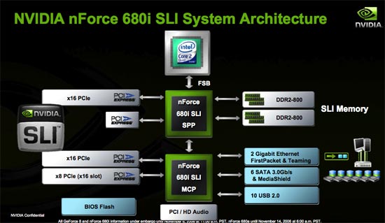
The 680i SLI is strictly a high end chipset, as the lower end of the market will still be serviced by NVIDIA's 570 SLI. The 680i supports all of the checkbox features: 1066MHz FSB (with unofficial support for higher speeds), dual channel DDR2-800, two PCIe x16 slots, one PCIe x8, 2 GbE ports, 6 SATA, 10 USB and HD Audio.
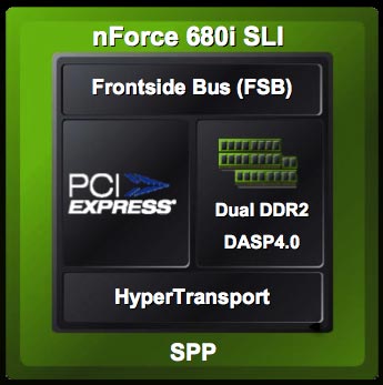
There are some pretty unique features about the new chipset. For starters it is the first NVIDIA core logic to be built on a 90nm process. The 680i SPP (aka North Bridge) is built on TSMC's 90nm process and thus ends up running cooler and can be overclocked more than NVIDIA's previous offerings in the area. The South Bridge (680i MCP) is still a 130nm chip but its functions are far less critical than those of the North Bridge.
In the 680i SPP is an updated version of NVIDIA's pre-fetching core called DASP. The major change to the 680i's DASP is that it is optimized for the memory access patterns of Conroe and Kentsfield which apparently are very different from NetBurst CPUs of the past. Given the aggressive prefetching done by the new Core processors and the large shared L2 cache, it isn't surprising to find out that memory controllers tuned to older Intel processors might not be best optimized for Core.
The primary function of the 680i's DASP is to examine memory access patterns and prefetch data into a local buffer that it thinks the processor will need at a later point in time. The updated version of DASP prefetches one cache line (64B) at a time into an internal buffer, although NVIDIA wouldn't disclose the size of the buffer.
We couldn't get much more information on DASP 4.0 from NVIDIA other than it supports prioritizing of reads over writes (to avoid read-to-write delays from random memory requests) and that a number of proprietary algorithms are used to make sure that prefetching doesn't occur when the CPU actually needs data from the memory controller.
Overclocking is a very large part of the new 680i chipset, and Wes' review of it goes into great detail about what exactly is possible with this new platform. For us, the other interesting part of the 680i platform is that, for the first time, NVIDIA is allowing its partners to sell NVIDIA engineered and designed 680i motherboards.
It has often been the case that a chipset maker's reference board has far more bells and whistles than anything its motherboard partners actually sell on the market. NVIDIA was growing weary of this being the case and instead effectively engineered a reference board that could be sold in retail.
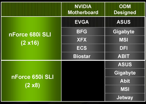
Motherboard makers can still choose to design their own 680i boards, but some have opted to simply rebrand NVIDIA's design.
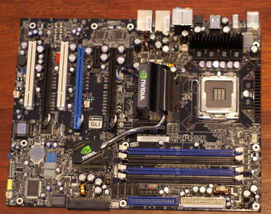
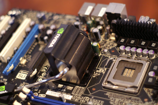
We ran all of our tests for this review on NVIDIA's nForce 680i SLI motherboard; this particular one is branded by EVGA. We were extremely pleased with the stability, BIOS, attention to detail and overall performance of the 680i solution. The decision to introduce NVIDIA designed 680i boards also shows how far NVIDIA has come as a manufacturer; if you want something done right, you sometimes have to do it yourself, and that's exactly what NVIDIA decided to do here. Honestly, the only downside is its estimated cost of $229.
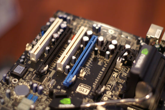
Three PCIe x16 slots (one is an x8 electrical)
NVIDIA is also introducing a lower cost 650i SLI chipset with only two x8 PCIe slots, but there will be no NVIDIA engineered boards available based on that chipset.


111 Comments
View All Comments
DerekWilson - Wednesday, November 8, 2006 - link
No DX10 for winxp -- but you've got OGL with extensions.We will certainly take a look at DX10 performance once we have DX10 apps.
Have fun glimpsing :-)