nForce 590 SLI Intel Edition: NVIDIA prepares an Intel 975X Killer
by Gary Key on June 27, 2006 6:15 AM EST- Posted in
- CPUs
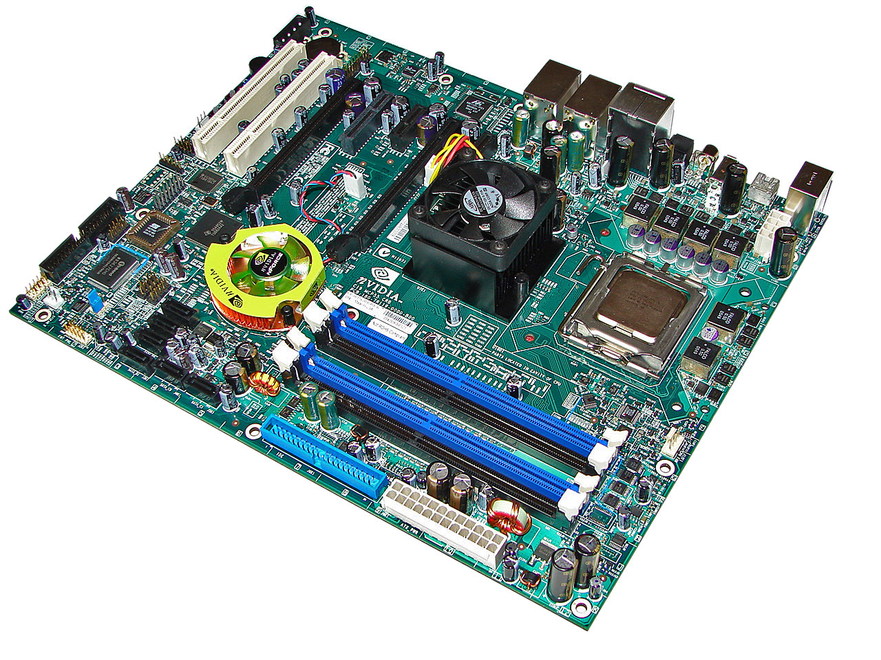
NVIDIA nForce 590 SLI: Reference Board Layout
NVIDIA designed a very well laid out board with all major connections easily reached. The board is lacking most clearance issues and was very easy to install in our mid-size ATX case. The reference board features an excellent voltage regulator power design along with Rubycon and Sanyo capacitors that yielded superb stability and overclocking results even with our early BIOS and board design.
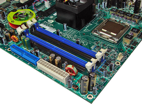
The DIMM module slots' color coordination is correct for dual channel setup based upon the premise of utilizing different colors for each memory bank. The memory modules are easy to install with a full size video card placed in the first PCI Express X16 slot. The 24-pin ATX power connector is located along the upper edge of the board along with the single IDE port connector.
The six NVIDIA SATA ports are color coded black and are conveniently located below the NVIDIA MCP. The SATA ports feature the newer clamp and latch design. We found the positioning of the SATA ports to be excellent when utilizing either PCI-E X16 slot. The NVIDIA MCP does require a heatsink in this application.
The floppy drive connector is color coded black while being positioned along the left edge of the board. The location of this connector is not ideal and actually the whole point of having a floppy drive connector is becoming moot with the wide spread availability of USB floppy or flash drives along with BIOS support for boot purposes. The various chassis panel, USB connectors, and the second chassis fan header are located in the lower left portion of the board.
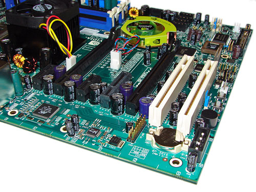
The board comes with (2) physical PCI Express X16 connectors, (1) PCI Express X1 connector, (1) PCI Express X4 connector, and (2) PCI 2.3 connectors. The layout of this design offers a very good balance of expansion slots for a mainstream board while providing excellent clearance space for graphics card utilization. Our main issue is that the first PCI 2.3 connector will be rendered physically useless if an SLI setup is utilized. Although the positioning and number of PCI-E and PCI slots are up to the manufacturer, we certainly hope to see better layouts that do not block the PCI slots in the near future. A four-pin molex power connector that is required for SLI operation and the first chassis fan header is located along the edge of the board. The four-pin molex connector is located in an unusual and difficult location to reach, the bottom left corner.
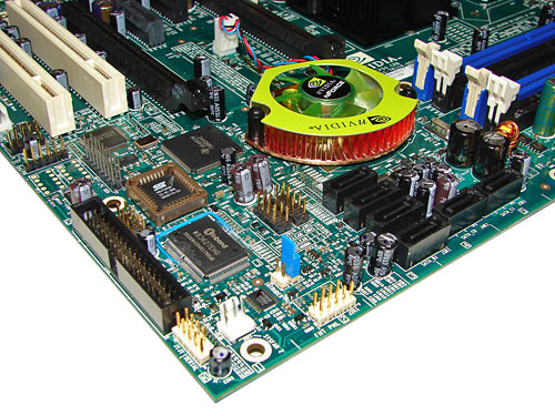
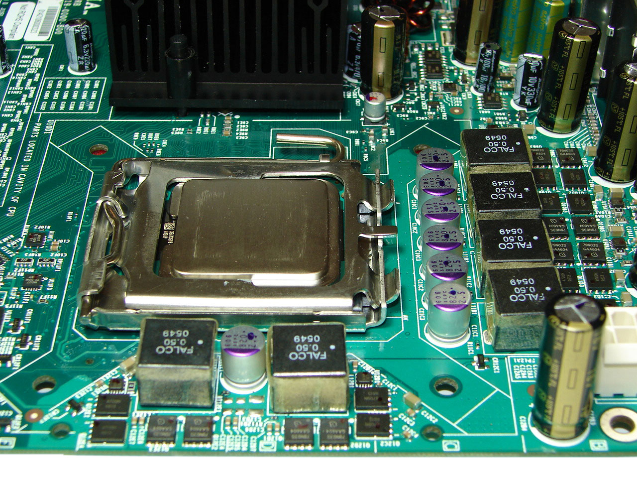
Returning to the CPU socket area, we find an ample amount of room for alternative cooling solutions. We utilized the stock heatsink/fan in our normal testing but also verified a couple of larger Socket 775 cooling solutions would fit in this area during our overclocking tests.
The NVIDIA SPP is actively cooled with a medium sized heatsink/fan unit that did not interfere with any installed peripherals. In fact this unit kept the chipset cool enough that additional chipset voltage was not a factor in our overclocking tests, although we could see this unit heating up if the HSF is not seated properly. Our only concern is the lifespan of the fan but it is very quiet during operation. NVIDIA places the 8-pin 12V auxiliary power connector at the top of the CPU socket area but out of the way of aftermarket cooling solutions.
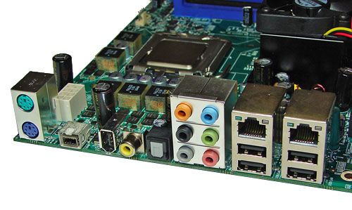
The rear panel contains the standard PS/2 mouse and keyboard ports, LAN ports, and 4 USB ports. The LAN (RJ-45) ports have two LED indicators representing activity and speed of the connection. The audio panel consists of 6 ports that can be configured for 2, 4, 6, and 8-channel audio connections. The rear panel also includes two S/PDIF (optical/coaxial) ports, an external SATA 3Gb/s port, and an IEEE 1394a port.
 |
| Click to enlarge |
NVIDIA designed a very well laid out board with all major connections easily reached. The board is lacking most clearance issues and was very easy to install in our mid-size ATX case. The reference board features an excellent voltage regulator power design along with Rubycon and Sanyo capacitors that yielded superb stability and overclocking results even with our early BIOS and board design.
The DIMM module slots' color coordination is correct for dual channel setup based upon the premise of utilizing different colors for each memory bank. The memory modules are easy to install with a full size video card placed in the first PCI Express X16 slot. The 24-pin ATX power connector is located along the upper edge of the board along with the single IDE port connector.
The six NVIDIA SATA ports are color coded black and are conveniently located below the NVIDIA MCP. The SATA ports feature the newer clamp and latch design. We found the positioning of the SATA ports to be excellent when utilizing either PCI-E X16 slot. The NVIDIA MCP does require a heatsink in this application.
The floppy drive connector is color coded black while being positioned along the left edge of the board. The location of this connector is not ideal and actually the whole point of having a floppy drive connector is becoming moot with the wide spread availability of USB floppy or flash drives along with BIOS support for boot purposes. The various chassis panel, USB connectors, and the second chassis fan header are located in the lower left portion of the board.
The board comes with (2) physical PCI Express X16 connectors, (1) PCI Express X1 connector, (1) PCI Express X4 connector, and (2) PCI 2.3 connectors. The layout of this design offers a very good balance of expansion slots for a mainstream board while providing excellent clearance space for graphics card utilization. Our main issue is that the first PCI 2.3 connector will be rendered physically useless if an SLI setup is utilized. Although the positioning and number of PCI-E and PCI slots are up to the manufacturer, we certainly hope to see better layouts that do not block the PCI slots in the near future. A four-pin molex power connector that is required for SLI operation and the first chassis fan header is located along the edge of the board. The four-pin molex connector is located in an unusual and difficult location to reach, the bottom left corner.
 |
| Click to enlarge |
Returning to the CPU socket area, we find an ample amount of room for alternative cooling solutions. We utilized the stock heatsink/fan in our normal testing but also verified a couple of larger Socket 775 cooling solutions would fit in this area during our overclocking tests.
The NVIDIA SPP is actively cooled with a medium sized heatsink/fan unit that did not interfere with any installed peripherals. In fact this unit kept the chipset cool enough that additional chipset voltage was not a factor in our overclocking tests, although we could see this unit heating up if the HSF is not seated properly. Our only concern is the lifespan of the fan but it is very quiet during operation. NVIDIA places the 8-pin 12V auxiliary power connector at the top of the CPU socket area but out of the way of aftermarket cooling solutions.
The rear panel contains the standard PS/2 mouse and keyboard ports, LAN ports, and 4 USB ports. The LAN (RJ-45) ports have two LED indicators representing activity and speed of the connection. The audio panel consists of 6 ports that can be configured for 2, 4, 6, and 8-channel audio connections. The rear panel also includes two S/PDIF (optical/coaxial) ports, an external SATA 3Gb/s port, and an IEEE 1394a port.


37 Comments
View All Comments
Frumious1 - Wednesday, June 28, 2006 - link
The problem is determining whether theres really a problem or the reviewers just need to learn how to use the motherboard and BIOS options properly. Wes, Gary, and most of the rest of the AnandTech crew seem to know how to really get results out of motherboards. I saw an article a few days ago that was an absolute joke when it comes to OCing. They took a 4200+ and were crowing about a 240 MHz HTT bus overclock or something. I don't think they ever even tried the other memory ratios.Anyway, registry corruption? Yeah, I've lost the registry a few times on Intel and AMD systems when pushing the OC a bit too far in the wrong way. Bad memory timings for an OC can be just as harmful as a bad CPU or chipset OC - probably even worse. OC'ing is not really that easy if you don't know what you're doing. Too many people want to just increase everything 25% and then tehy wonder why the system won't POST.
Someone on AT did some OCing articles last year about the topic that really provided some good details, showing 2.6 GHz or so with an X2 3800+ using everything from POS value RAM up through top quality TCCD and CH5 modules. Probably took a hell of a long time to complete all the testing as well! If you want to do a motherboard review right and you want to look at overclocking, you simply can't do that without spending a good month or more with the board. Sometimes a seemingly small change will stabilize what appeared to be a hopeless OC.
Bottom line: if you want SLI (and honestly, for dual GPUs it's far better than CrossFire right now - maybe not in performance, but the ATI CF drivers are still crap!) for Conroe, you'll need an nVidia chipset. Unless they suddenly get with the program and start supporting SLI on any dual X16 slot board? God, wouldn't that be nice? Stupid political bullshit... from nVidia and ATI!
Frumious1 - Wednesday, June 28, 2006 - link
Dammit... I did it again and used an H in brackets... which turns on white text for reasons unknown. Repost so people can read the text without highlighing:--------------
The problem is determining whether theres really a problem or the reviewers just need to learn how to use the motherboard and BIOS options properly. Wes, Gary, and most of the rest of the AnandTech crew seem to know how to really get results out of motherboards. I saw a HardOCP article a few days ago that was an absolute joke when it comes to OCing. They took a 4200+ and were crowing about a 240 MHz HTT bus overclock or something. I don't think they ever even tried the other memory ratios.
Anyway, registry corruption? Yeah, I've lost the registry a few times on Intel and AMD systems when pushing the OC a bit too far in the wrong way. Bad memory timings for an OC can be just as harmful as a bad CPU or chipset OC - probably even worse. OC'ing is not really that easy if you don't know what you're doing. Too many people want to just increase everything 25% and then tehy wonder why the system won't POST.
Someone on AT did some OCing articles last year about the topic that really provided some good details, showing 2.6 GHz or so with an X2 3800+ using everything from POS value RAM up through top quality TCCD and CH5 modules. Probably took a hell of a long time to complete all the testing as well! If you want to do a motherboard review right and you want to look at overclocking, you simply can't do that without spending a good month or more with the board. Sometimes a seemingly small change will stabilize what appeared to be a hopeless OC.
Bottom line: if you want SLI (and honestly, for dual GPUs it's far better than CrossFire right now - maybe not in performance, but the ATI CF drivers are still crap!) for Conroe, you'll need an nVidia chipset. Unless they suddenly get with the program and start supporting SLI on any dual X16 slot board? God, wouldn't that be nice? Stupid political bullshit... from nVidia and ATI!
Anemone - Wednesday, June 28, 2006 - link
You certainly make good points. However one review of "good" and many, many of "bad" doesn't lead me to think the "good" just knew what they were doing. In fact it's quite the opposite. It leads me to think they didn't dig deep enough.Gary Key - Friday, June 30, 2006 - link
I will take a different path on this one. We were allowed a first look at the board with Conroe back in early May, in fact if we could have stayed an extra day we would have had significant hands-on time with the setup. We were also one of the first sites to receive a board from NVIDIA for the specific purpose of testing the board to provide specific feedback regarding Conroe compatibility and performance. I easily have over 200 hours of test time on this board along with a couple of pages of issues/improvements/suggestions we would like to see before the design goes into production. As far as not digging deep enough, I doubt we would have had this early of an opportunity if it were not for our work (and that of several AT readers) with NVIDIA over the past several months in assisting them and the board suppliers to get their Intel performance up to speed. We are still very disappointed with the FSB overclocking results with the NVIDIA Intel designs but our initial board had no issue running up to 304FSB with an early Conroe sample. I am personally disappointed with the entire FSB issue since last fall as I had a couple of boards that easily did over 320FSB only to see this capability whacked when the product was released.
Yes, the board will use the nF4 SLI SPP for the "Northbridge" but it is now at a C1 stepping after several months of tuning due to the issues found last fall in the first release. Are we disappointed that we will not get the newer C51XE SPP, yes, but the time to develop it along with the switch to a single dual x16 chipset this winter made it impractical for NVIDIA at this time. The good news is the NV590SLI boards should cost around $150 at launch with a feature set that will not be matched by Intel or ATI along with using the new MCP55PXE so drive and network performance is greatly improved from a stability viewpoint.
We did not post the actual memory scores as we are waiting on a new board revision and production level bios before making any final statements on this subject and FSB overclocking. However, even with the 805D the base unbuffered Sandra scores were about 2% better than the i975x. When overclocked, this margin flipped in favor of the Intel board. The margin was even greater during our Conroe testing. I am still concerned with the FSB overclocking capability. I stated this at the end of the article, it is a concern and will remain a concern until we see production level boards. I think it will improve compared to today's products but I doubt we will see anything near what the i975x and now P965 chipsets will be capable of in the high end boards from Asus, DFI, Abit, MSI, and Gigabyte. However, getting over 300FSB is a requirement we have placed on NVIDIA at this time. It will be interesting to see if they can get there now.
We appreciate the comments and please keep them coming. Our final review on the reference board will be available shortly and we should have boards from DFI and Asus around Core 2 Duo launch time. However, we do not expect ATI review samples until sometime in August along with some interesting information about their design choice that will be discussed at that time.
mino - Tuesday, June 27, 2006 - link
Almost every p$ chipset capable of 10066 FSB since i865 tiems DOES support Conroes. Just crippled Intel 915/925 series do NOT bute even this is caused by intel marketing decision not the capability of chipset design on itself.What is most important is the board/VRM support. Otherwise every not-crippled chipset should work.
mino - Tuesday, June 27, 2006 - link
P4 meant :)mino - Tuesday, June 27, 2006 - link
hell, I should get some sleep apparently ;-\