Out of Order execution: AMD versus Intel
To make this article more accessible and to make the differences between the AMD K8 and the new Intel Core architecture more clear, I tried to make both CPU diagrams in the same style. Here's the Core architecture overview: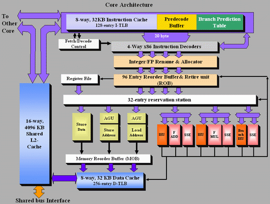
And here's the K8 architecture:
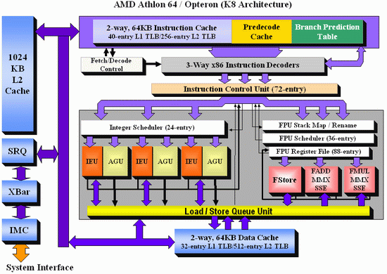
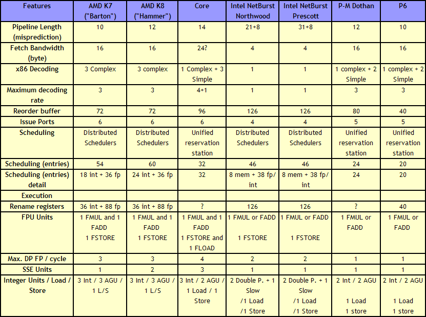
There are a few obvious differences: Core has bigger OoO buffers: the 96 entry ROB buffer is - also thanks to Macro-op fusion - quite a bit bigger than the 72 Entry Macro-op buffer of K8. The P6 architecture could order only 40 instructions, this was doubled to 80 in the P-M architecture (Banias, Dothan, Yonah), and now it's increased even further to 96 for the Core architecture. We've created a table which compares the most important architectural details of several current CPU families:
 |
| Click to enlarge |
The Core architecture uses a central reservation station, while the Athlon uses distributed schedulers. The advantage of a central reservation station is that utilization is better, however distributed schedulers allow more entries. NetBurst also uses distributed schedulers.
Using a central reservation station is another clear example of how Core is in fact the "P8", the second big improvement of the P6 architecture. Just like the P6 architecture, it uses a Reservation Station (RS) and allocates a specific execution unit to execute the micro-op. After execution, the micro-op results are stored in the ROB entry for that micro-op. This aspect of the Core design is clearly taken from the Yonah, Dothan and P6 architectures.
The biggest differences are not immediately visible on the diagrams above. Previous Intel architectures can only perform one branch prediction every two cycles, but Core can sustain one branch per cycle. The Athlon 64 can also perform one branch prediction per cycle.
Another impressive area is Core's SSE multimedia power. Three very powerful 128-bit SSE/SSE2/SSE3 units are available, and two of them are symmetric. Core will outperform the Athlon 64 vastly when it comes to 128-bit SSE2/3 processing.
On K8, 128-bit SSE instructions are decoded into two separate 64-bit instructions. Each Athlon 64 SSE unit can only do one 64-bit instruction at a time, so the Core architecture has essentially at least 2 times the processing power here. With 64-bit FP, Core can do 4 Double Precision FP calculations per cycle, while the Athlon 64 can do 3.
When it comes to integer execution resources, the Core architecture is an improvement over the Pentium 4 and Dothan CPUs, and is at the same level (if we only look at the number of execution units) as the Athlon 64. The Athlon 64 seems to have a small advantage when it comes to calculating addresses: it has 3 AGU compared to Core's 2. This could give the Athlon 64 an advantage in some less common integer workloads such as decrypting algorithms. The deeper, more flexible (Memory disambiguation, see further) out of order buffers and bigger, faster L2-cache of the Core should negate this small advantage in most integer workloads.


87 Comments
View All Comments
spinportal - Monday, May 1, 2006 - link
Definitely a great treasure of an article to find on a monday morning detailing the Core architecture that the world is drooling for in June. I wonder what kind of simulation micro-arch software Intel and AMD use, as I remember the days doing my Masters, playing with Intel's Hypercube simulator (grav sim, fish & shark AI sim) and writing my own macro level visual-cpu execution simulator.JarredWalton - Monday, May 1, 2006 - link
I won't say it's a quick fix, but just as Core is a derivative of P6, AMD could potentially just get some better OoO capabilities into K8 and get some serious performance improvements. Their current inability to move loads forward much (if at all) makes them even more dependent on RAM latency. You could even say that they *needed* the IMC to improve performance, but still L2 latency is far better than RAM latency, and cutting down L2 latency hit from 12 cycles to say 6 cycles (if you can do the load 6 cycles early) would have to improve performance. Loads happen "all the time" in ASM, so optimizing their performance can pay huge dividends.I'm going to catch flak for this, but basically Intel has more elegant designs than AMD in several areas. It comes from throwing billions of dollars at the problems. Better L1 cache? Yup - 8-way vs. 2-way is pretty substantial; 256-bit vs. 128-bit is also substantial. Better specialization of hardware? Yeah, I have to give them that as well: rather than just using three ALUs, they often take the path of having a few faster ALUs to handle the common cases.
Really, the only reason AMD was able to catch (and exceed) Intel performance was because Intel got hung up on clock speeds. They basically let marketing dictate chip design to engineering - which is never good, IMO, at least not in the long run. Even NetBurst still has some very interesting design features (double-pumped ALUs, specialization of functional units, trace cache), and if nothing else it served as a good lesson on how far you can push clock speeds and pipeline lengths before you start encountering some serious problems. I would have loved to see Northwood tweaked for 90nm and 65nm, personally - 31+8 pipeline stages was just hubris, but 20+8 with some other tweaks could have been interesting.
Here's hoping AMD can make some real improvements to their chips sooner rather than later. Intel Core is looking very strong right now, and I would rather have close competition than a 20% margin of victory like we've been seeing lately. (First with AMD K8 beating NetBurst, and now it looks like Conroe is going to turn the tables.)
Regs - Wednesday, June 7, 2006 - link
Okcourse you will catch flack. It's an opinion.My opinion is Intel is more innovative or even compromising
while AMD is more intuitive.
Spoonbender - Monday, May 1, 2006 - link
"8-way 32kb * 2 L1 should in theory exceed the hitrate of K8's 2-way 64kb * 2 L1."It should? I'd like to see some sources on that. From what I've seen, the 64KB cache still has an advantage there, with a hitrate not much below that of a 64KB/8-way.
Also, I disagree that Intel's CPU's are generally more elegant. First, their L1 cache isn't neccesarily "better" (see above). Of course, the 256 vs 128 bit bandwidth is a big factor, however.
Specialization in hardware? Is that elegant? I'd say there's a certain elegance in making a general solution as well, as opposed to specializing everything to the point where you're screwed if the code you have to execute isn't 100% optimal.
And I definitely think AMD's distributed reservation stations are more elegant than the central one used by Intel. Same goes with the usual HyperTransport vs FSB story.
There are a few other really elegant features of the K8 that I haven't seen duplicated in Core.
So overall, I don't see the big deal with "elegance". Both architectures have plenty of elegant features. However, the K8 is definitely aging, and will have problems keeping up with Conroe.
But then again, the K8 die is tiny in comparison. They've got plenty of space for improvements.
Really looking forward to
1) Being able to get a Merom-powered laptop, and
2) Seeing what AMD comes up with next year.
IntelUser2000 - Monday, May 1, 2006 - link
Tiny?? 199mm2 for 2x1MB cache K8 at 90nm is tiny?? Ok there. Conroe with 4MB cache is around 140mm2 die size.
http://www.aceshardware.com/forums/read_post.jsp?i...">http://www.aceshardware.com/forums/read_post.jsp?i...
Even compairing against Intel's SRAM size for 90nm and 65nm comparison, at 90nm, Conroe would be 250mm2. In Prescott, 1MB L2 cache takes 16-17mm2. 250mm2-32mm2=218mm2.
And Intel didn't to shrinks that are relative to SRAM sizes. In comparison for Cedarmill and Prescott 2M, which are same cores essentially.
Prescott 2M: 135mm2
Cedarmill: 81mm2
Only difference being process size, the comparison is 0.6.
Conroe at 90nm would have been 233mm2, which is compact as X2 per core.
Spoonbender - Tuesday, May 2, 2006 - link
Okay, I guess I should have said that at the same process size, it is tiny. I meant that when AMD gets around to migrating to 65nk as well, they'll have a smaller core (assuming no big changes to the chip), which gives them plenty (some?) of room for improvement.[quote]
Conroe at 90nm would have been 233mm2, which is compact as X2 per core.
[/quote]
But in absolute terms, still bigger than an Athlon X2. Which means AMD has some space for improvement. That was my only point. I guess I should have been more clear. ;)
coldpower27 - Wednesday, May 3, 2006 - link
Yes, if using the 0.6 Factor for Brisbane the 65nm Athlon 64x2 it will be around 132mm2 assuming no changes over the 220mm2 Windsor DDR2 Athlon64x2. 199mm2 is only for Toledo which is reaching end of life and can no longer be used as a comparison. And it's irrelevent to compare to Conroe on what it would be on 90nm as it never was built on 90nm technology to begin with.Conroe is looking to be ~14x mm2 with the x=0-9. Yes if you can compare them at the same process nodes considering the Conroe will only be competing with the 65nm Dual Core Athlon 64x2 in the second half of it's lifetime.
JumpingJack - Tuesday, May 2, 2006 - link
Nice analysis, the current AMD X2 dual cores are about 1.5 to 2.0 X the size of Intel dual cores (on 65 nm), this is where 65 nm adds such a benefit. Conroe will come in around 140 mm^2 as you said. Yohna at 2 meg shared is 90 mm^2, less than 1/2 the X2.Right now, cost wise in Si realestate AMD is more expensive.
BitByBit - Monday, May 1, 2006 - link
Here is a good article on processor cache:
http://en.wikipedia.org/wiki/CPU_cache">http://en.wikipedia.org/wiki/CPU_cache
If you scroll down to the miss-rate vs. cache size graph, you can see that an 8-way 64Kb cache has a miss-rate less than one-tenth the miss-rate of a 2-way 64Kb cache.
An 8-way 64Kb * 2 L1 would probably be too difficult to implement, given the time it would take to search. However, according to the relationships shown by that graph, increasing the Athlon's L1 associativity to 4-ways could yield a nice boost in hitrate and consequently performance.
Spoonbender - Monday, May 1, 2006 - link
And of course, we all know wikipedia is the ultimate source of all truth and knowledge... ;)Keep in mind that this graph only shows the Spec2000 benchmark (and only the integer section, at that). That's far from being representative of all code.
According to http://www.amazon.com/gp/product/1558605967/002-28...">http://www.amazon.com/gp/product/155860...-2818646... which, in my experience is pretty damn good, the missrates are as follows *in general*:
32KB, 8-way: 0.037
64KB, 2-way: 0.031
64KB 8-way: 0.029
But yeah, of course improving the Athlon's cache would help. But it's not the first place I'd look to optimize. For one thing, making it more complex would, as seen above, not yield a significantly lower hitrate, but it would slow the cache down, either forcing them to increase its latency, or limiting the frequency potential of the cpu as a whole. The cache bandwidth might be a better candidate for improvement. Or some of the actual cpu logic. Or the L2 cache size. I think the L1 cache is pretty healthy on the K8 already.