Smarter Decoding
Similar to the K8 architecture, Core pre-decodes instructions that are fetched. Pre-decode information includes instruction length and decode boundaries.A first for the x86 world, the Core architecture is equipped with four x86 decoders, 3 simple decoders and 1 complex decoder. The task of the decoders - for all current x86 CPUs - is not only to decipher the incoming instruction (opcode, addresses), but also to translate the 1 to 15 byte variable length x86 instructions into - easier to schedule and execute - fixed length RISC-like instructions (called micro-ops).
The most common x86 instructions are translated into a single micro-op by the 3 simple decoders. The complex decoder is responsible for the instructions that produce up to 4 micro-ops. The really long and complex x86 instructions are handled by a microcode sequencer. This way of handling the complex most CISC-y instructions has been adopted by all modern x86 CPU designs, including the P6, Athlon (XP and 64), and Pentium 4.
There is still more to the Core decoders. The first clever technique is macro-op fusion. It makes it possible for two relatively common x86 instructions to be fused into a single instruction. For example, the x86 compare instruction (CMP) is fused with a jump (JNE TARG). These instructions are typically the assembler result of a compiled if-then-else statement.
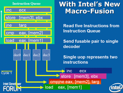
The result is that on average in a typical x86 program, for every 10 instruction, two x86 instructions (called macro-ops by Intel) are fused together. When two x86 instructions are fused together, the 4 decoders can decode 5 instructions in one cycle. The fused instruction travels down the pipeline as a single entity, and this has other advantages: more decode bandwidth, less space taken in the Out of Order (OoO) buffers, and less scheduling overhead. If Intel's "1 out of 10" claims are accurate, macro-ops fusion alone should account for an 11% performance boost relative to architectures that lack the technology.
The second clever technique already exists in the current P-M CPUs. There are a few x86 instructions which are pretty complex to perform, but which are at the same time a very typical and common x86 instruction. We are talking for example about mathematical operations where an address is referenced instead of a register. One common example is ADD [mem], EAX . This means add the content of register EAX to the content of a certain memory location (i.e. store the result back at the memory address). Store instructions which get broken down into store address and store data are another example.
In earlier designs such as the P6 (Pentium Pro, PII, PIII) architecture, these instruction would have been broken up into two or even three micro-ops. Remember that the whole philosophy behind all modern x86 CPUs, since the P6, is to decode x86 instructions into RISC-y micro-ops which are then fed to a fast RISC backend; the backend then schedules, issues, executes and retires the instructions in a smooth RISC way.
There is no way you could feed such an instruction (ADD [mem], EAX) to RISC execution units. It violates every RISC rule. RISC designs all load their data into the registers and then perform the necessary calculation on the registers.
So ADD [mem], EAX is broken down into:
Load the contents of [mem] into a register (Since Banias, the ALU and the Load operation are kept together in one micro-op. This is called micro-op fusion. This is no small feat: in older designs keeping the load and ALU operation together would result in pipeline stages that take much longer and thus lower the maximum clock frequency. (In CPU designs, the maximum clock speed is essentially determined by the slowest possible pipeline stage execution time.) Only by using bigger, smarter circuitry that can do a lot in parallel is micro-op fusion possible without lowering the clock speed significantly.MOV EBX, [mem])
An ALU operation, ADD the two registers together (ADD EBX, EAX)
Store the result back to memory (MOV [mem], EBX)
The pre-decode stage recognizes the macro-ops (or x86) instructions that should be kept together. In the decoding phase, ADD [mem], EAX results in one micro-op. Again, this means that the CPU can stuff more instructions in the same OoO buffers, increasing efficiency and improving performance.
Core versus Hammer: Decoding
All very nice, but let us take a look at what really matters: How do the 3 simple + 1 complex decoders of Core compare to the 3 complex decoders of AMD's K8 architecture?The original Athlon ("K7") has two way of decoding, Vector and Direct Path. The Vector Path decoding results in more than two RISC-like instructions (called "macro-ops" by AMD), the Direct Path in one, sometimes two macro-ops. Each of the decoders in K7 can handle both Vector Path and Direct Path decoding, but from a performance standpoint Direct Path is preferred since it results in fewer macro-ops. If you're wondering why were discussing K7 all of a sudden, just as Core is largely based off the P6 architecture, K8 is largely based off the K7 architecture.
The 3 complex decoders are powerful and can decode most x86 instructions, with few instructions requiring the Vector Path. The only downside of the K7 decoders is that some FP instructions and SSE instructions have to pass through the Vector Path. K8 has even stronger complex decoders and almost all FP and SSE instructions are also now decoded through the Direct Path decoders. This is possible as fetching and decoding takes more stages than it did in the K7; the K8 architecture is clearly more powerful when it comes to SIMD.
Obviously, Intel's Macro-op ( x86 instruction ) fusion does not exist in AMD's K8. However, micro-op fusion is available in another form. If we compare Intel's and AMD's macro-ops and micro-ops, it is easy to get confused. Take a look at the table below which explains the differences.
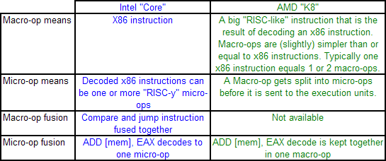
Micro-op fusion does exist in the Athlon. An ADD [mem], EAX is kept together in one macro-op as it travels through the pipeline. Therefore it will take only one place in the OoO buffers. However, the load and execute SSE/SSE2 operations can be fused on Core, while this is not the case on K8: packed SSE operations result in two macro-ops.
So how do Intel's Core and AMD's Hammer compare when it comes to decoding? It is hard to say at the moment without access to Intel's optimization manuals. However, we can get a pretty good idea. In almost every situation, the Core architecture has the advantage. It can decode 4 x86 instructions per cycle, and sometimes 5 thanks to x86 fusion. AMD's Hammer can do only 3.
The situation where AMD's 3 complex decoders can outperform Core's 1 complex + 3 simple decoders is much less likely to happen. It would happen when 3 instructions would be fetched that would have to be handled by the complex decoder of the Core CPU, but which are not too complex that the Microcode Sequencer must kick in. Since the most used x86 instructions all map to one Intel micro-op, this is pretty unlikely.


87 Comments
View All Comments
BigT383 - Monday, May 1, 2006 - link
I loved this article. It's due to articles like these that I've been reading Anandtech since before the days of the K6-2.PandaBear - Monday, May 1, 2006 - link
Of course Core should be better than K8, it better be.The only thing I am concerned about the Core architecture is with all these additional stuff, it will probably cost a lot to make, not just the CPU, but the MB, chipset, will also be expensive with the additional high speed circuitry. That means it will probably cost more.
K8 has been 5 years old and it is not bad standing against the latest and greatest. If AMD have something in the pipeline that will be the next monster CPU, it will be great. What I am concern about AMD is whether they can keep their yield up and have enough $ left behind to design K9 and beyond. Don't just sit there and lose the momentum they gain.
saratoga - Monday, May 1, 2006 - link
Core is a pretty conservative design with a pretty small die for a new core. It should be very economical to produce. Probably more so then the chips its replaceing.IntelUser2000 - Monday, May 1, 2006 - link
Not really. Not many expected that Intel will do more than increasing clock speeds and cache sizes since that's what they have been doing that since Pentium II.
http://www.reghardware.co.uk/2006/04/05/intel_conr...">http://www.reghardware.co.uk/2006/04/05/intel_conr...
The ASP went down. $530 for the fastest mainstream Conroe is rather good.
zsdersw - Monday, May 1, 2006 - link
The pricing put out by Intel suggests that Core will be priced very aggressively. I can't see the 975 chipset costing significantly more than it does now when Core is released.The fact that Core is going to be built on Intel's 65nm process means that the "additional stuff" you refer to will cost less than it would if built on the 90nm process. And the die size probably grew a little, but not enough to offset the cost gains from the 65nm process.
xtremejack - Monday, May 1, 2006 - link
K8 is only 3 years old. Didn't AMD celebrate their 3rd anniversary of Opteron a few days ago.Griswold - Thursday, May 4, 2006 - link
Its been sold for 3 years, but clearly the design is "a few days" older than that.evident - Monday, May 1, 2006 - link
as a junior computer engineer at villanova university, i found this article to be really informative and an awesome read. it's really cool to see the differences between these CPU architectures and shows that they are actually teaching me something useful!PeteRoy - Monday, May 1, 2006 - link
How can you say Netburst wasn't a huge success?I think Netburst was a success when it was launched and it should have died sooner, but it was good for it time and now it will be replaced.
JarredWalton - Monday, May 1, 2006 - link
NetBurst started at 1.5 GHz basically and topped out at 3.8 GHz. Compared to previous architectures, that's pretty tame. P6 went from 150 MHz to 1.26 GHz (and beyond if you want to count P-M). Success monetarily vs. success as an overall design are two different things, and clearly NetBurst ran into trouble. Where are the 5 GHz+ Tejas chips? Waiting somewhere beyond the thermal even horizon.... :)