Smarter Decoding
Similar to the K8 architecture, Core pre-decodes instructions that are fetched. Pre-decode information includes instruction length and decode boundaries.A first for the x86 world, the Core architecture is equipped with four x86 decoders, 3 simple decoders and 1 complex decoder. The task of the decoders - for all current x86 CPUs - is not only to decipher the incoming instruction (opcode, addresses), but also to translate the 1 to 15 byte variable length x86 instructions into - easier to schedule and execute - fixed length RISC-like instructions (called micro-ops).
The most common x86 instructions are translated into a single micro-op by the 3 simple decoders. The complex decoder is responsible for the instructions that produce up to 4 micro-ops. The really long and complex x86 instructions are handled by a microcode sequencer. This way of handling the complex most CISC-y instructions has been adopted by all modern x86 CPU designs, including the P6, Athlon (XP and 64), and Pentium 4.
There is still more to the Core decoders. The first clever technique is macro-op fusion. It makes it possible for two relatively common x86 instructions to be fused into a single instruction. For example, the x86 compare instruction (CMP) is fused with a jump (JNE TARG). These instructions are typically the assembler result of a compiled if-then-else statement.
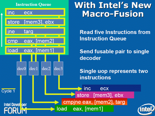
The result is that on average in a typical x86 program, for every 10 instruction, two x86 instructions (called macro-ops by Intel) are fused together. When two x86 instructions are fused together, the 4 decoders can decode 5 instructions in one cycle. The fused instruction travels down the pipeline as a single entity, and this has other advantages: more decode bandwidth, less space taken in the Out of Order (OoO) buffers, and less scheduling overhead. If Intel's "1 out of 10" claims are accurate, macro-ops fusion alone should account for an 11% performance boost relative to architectures that lack the technology.
The second clever technique already exists in the current P-M CPUs. There are a few x86 instructions which are pretty complex to perform, but which are at the same time a very typical and common x86 instruction. We are talking for example about mathematical operations where an address is referenced instead of a register. One common example is ADD [mem], EAX . This means add the content of register EAX to the content of a certain memory location (i.e. store the result back at the memory address). Store instructions which get broken down into store address and store data are another example.
In earlier designs such as the P6 (Pentium Pro, PII, PIII) architecture, these instruction would have been broken up into two or even three micro-ops. Remember that the whole philosophy behind all modern x86 CPUs, since the P6, is to decode x86 instructions into RISC-y micro-ops which are then fed to a fast RISC backend; the backend then schedules, issues, executes and retires the instructions in a smooth RISC way.
There is no way you could feed such an instruction (ADD [mem], EAX) to RISC execution units. It violates every RISC rule. RISC designs all load their data into the registers and then perform the necessary calculation on the registers.
So ADD [mem], EAX is broken down into:
Load the contents of [mem] into a register (Since Banias, the ALU and the Load operation are kept together in one micro-op. This is called micro-op fusion. This is no small feat: in older designs keeping the load and ALU operation together would result in pipeline stages that take much longer and thus lower the maximum clock frequency. (In CPU designs, the maximum clock speed is essentially determined by the slowest possible pipeline stage execution time.) Only by using bigger, smarter circuitry that can do a lot in parallel is micro-op fusion possible without lowering the clock speed significantly.MOV EBX, [mem])
An ALU operation, ADD the two registers together (ADD EBX, EAX)
Store the result back to memory (MOV [mem], EBX)
The pre-decode stage recognizes the macro-ops (or x86) instructions that should be kept together. In the decoding phase, ADD [mem], EAX results in one micro-op. Again, this means that the CPU can stuff more instructions in the same OoO buffers, increasing efficiency and improving performance.
Core versus Hammer: Decoding
All very nice, but let us take a look at what really matters: How do the 3 simple + 1 complex decoders of Core compare to the 3 complex decoders of AMD's K8 architecture?The original Athlon ("K7") has two way of decoding, Vector and Direct Path. The Vector Path decoding results in more than two RISC-like instructions (called "macro-ops" by AMD), the Direct Path in one, sometimes two macro-ops. Each of the decoders in K7 can handle both Vector Path and Direct Path decoding, but from a performance standpoint Direct Path is preferred since it results in fewer macro-ops. If you're wondering why were discussing K7 all of a sudden, just as Core is largely based off the P6 architecture, K8 is largely based off the K7 architecture.
The 3 complex decoders are powerful and can decode most x86 instructions, with few instructions requiring the Vector Path. The only downside of the K7 decoders is that some FP instructions and SSE instructions have to pass through the Vector Path. K8 has even stronger complex decoders and almost all FP and SSE instructions are also now decoded through the Direct Path decoders. This is possible as fetching and decoding takes more stages than it did in the K7; the K8 architecture is clearly more powerful when it comes to SIMD.
Obviously, Intel's Macro-op ( x86 instruction ) fusion does not exist in AMD's K8. However, micro-op fusion is available in another form. If we compare Intel's and AMD's macro-ops and micro-ops, it is easy to get confused. Take a look at the table below which explains the differences.
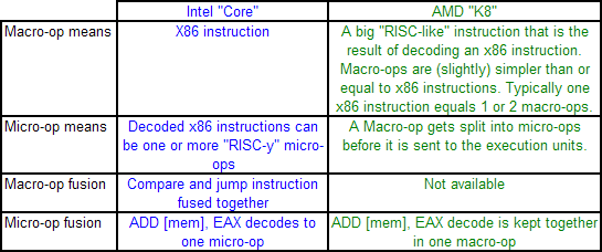
Micro-op fusion does exist in the Athlon. An ADD [mem], EAX is kept together in one macro-op as it travels through the pipeline. Therefore it will take only one place in the OoO buffers. However, the load and execute SSE/SSE2 operations can be fused on Core, while this is not the case on K8: packed SSE operations result in two macro-ops.
So how do Intel's Core and AMD's Hammer compare when it comes to decoding? It is hard to say at the moment without access to Intel's optimization manuals. However, we can get a pretty good idea. In almost every situation, the Core architecture has the advantage. It can decode 4 x86 instructions per cycle, and sometimes 5 thanks to x86 fusion. AMD's Hammer can do only 3.
The situation where AMD's 3 complex decoders can outperform Core's 1 complex + 3 simple decoders is much less likely to happen. It would happen when 3 instructions would be fetched that would have to be handled by the complex decoder of the Core CPU, but which are not too complex that the Microcode Sequencer must kick in. Since the most used x86 instructions all map to one Intel micro-op, this is pretty unlikely.


87 Comments
View All Comments
Betwon - Wednesday, May 3, 2006 - link
If you really want to know what is the Intel's load reordering and memory misambiguation, I can tell you the facts:http://www.stanford.edu/~merez/papers/LoadSched_IS...">http://www.stanford.edu/~merez/papers/LoadSched_IS...
Speculation Techniques for Improving Load Related Instruction Scheduling 1999
Adi Yoaz, Mattan Erez, Ronny Ronen, and Stephan Jourdan -- From Intel's Haifa, they designed the Load/Store Unit of Core.
I had said that anandtech should study many things about CPU. Of course, I should study more things about CPU.
Betwon - Tuesday, May 2, 2006 - link
P6: sub [mem],eax decodes to three micro-opsCore duo: sub [mem],eax decodes to two micro-ops
K8: sub [mem],eax decodes to one macro-op
P6: sub eax,[mem] decodes to two micro-ops
Core duo: sub eax,[mem] decodes to one micro-op
K8: sub eax,[mem] decodes to one macro-op
Intel's micro-fusion is different with the K7/K8's macro-op.
P4 has 2X2 int ALU and 2 AGU.
K7/K8 has 3 int ALUand 3 AGU.
But Core duo has only 2 int ALU and 2 AGU.
The integer performance:
Core duo>K7/K8
Why?
Because Core duo's length of the depenency chain of the critical path is the shorest.
The most integer program asm codes can be thought as a high and thin tree of the depenency chain, (the longest depenency chain is called the critical path)
The critical path determines the performance. The length of the depenency chain of the critical path is the cycles needed to complete this critical path.
Core duo(2ALU/2AGU) spends less cycles than K7/K8(3ALU/3AGU) -- Because more INT funtions can not accelerate the true dependency atoms-operations.
The P-M/Core duo's special ability of anti true dependency atoms-operations is the real reason of it's INT outperformance, which is different with old P6(such as Pentium 3).
The most FP program asm codes can be thought as a boskage (there are many short depenency chains). The best ILP can be performed--The more FP FADD/FMUL funtions, the more performence.
Double the FP funtions or double the speed of half-speed FP functions is a good idea for the most FP programs.
But double INT funtions do not always enhence the INT preformence so greatly.
Conroe only has three ALUs and two AGUs, but not 4 ALU and 4AGU.
K7/K8 has three ALUs and three AGUs.
Betwon - Tuesday, May 2, 2006 - link
Sorry, I'm not one from a English-language nations. I just tell my idea with many spelling or syntax errors.funtions -- funtion units
I want to tell why Conroe with only 3ALU/2AGU has the INT outperformance. Core has the superexcellent ability to process the true dependency chains.(much much better than K8 3ALU/3AGU).
Even Core duo with 2ALU/2AGU has the INT outperformance(much better than K8 3ALU/3AGU).
The length of the depenency chain of the critical path
The true dependency atom-operations
Starglider - Monday, May 1, 2006 - link
A truly excellent article. I just have a couple of questions;It's clear that increasing FSB speed can reduce memory latency. However I'm not clear why lower CPU core speed will reduce absolute latency - sure it will reduce the number of CPU cycles that occur while waiting for memory, but how can it reduce the absolute delay?
You don't seem to have included inter-instruction latency in your comparison tables. I know this data can be hard to get hold of, but it's critical to the performance of highly serial code (e.g. the pi calculation benchmarks that seem to be so popular at the moment). Is there any chance it could be included?
Finally I'm wondering if Intel will revist some of the P4 clock speed enhancing tricks later on. Things like LVS and double pumped AUs would only have slowed down an already complex development process that Intel desperately needed to be completed quickly. But if AMD do come out with a new architecture that matches or exceeds Conroe on IPC, Intel might be able to respond quite quickly by bringing back some of their already well understood clock speed tricks to accelerate Conroe.
Makaveli - Monday, May 1, 2006 - link
You need to get away from thinking of increased clockspeed for extra performance, the future is multicore Cpu's and parellism.Starglider - Tuesday, May 2, 2006 - link
I write heavily multithreaded applications for a living, but sometimes there is just no substitute for fast serial execution; a lot of things just can't be parallelised. Serial execution speed is effectively IPC * clock rate, so yes increasing clock rate is still very helpful as long as IPC doesn't suffer.saratoga - Monday, May 1, 2006 - link
^^ Did you read the post you replied to? His point is valid.Lower clock speed is not going to improve memory latency. It may mean that latency is less painful, but if you took two core chips, one at 2GHz and the other at 3GHz, the absolute latency is roughly if not exactly the same for each. Though the cost of each ns of latency is 50% more dear on the 3GHz chip.
Spoonbender - Tuesday, May 2, 2006 - link
It would be more accurate to say that each cycle of latency is more dear on the 2ghz chip, wouldn't it? ;)What matters is how *long* the latency is, in ns. A ns latency is a ns, and it forces the cpu to wait exactly one ns, no matter its clock speed... :)
So yeah, definitely a valid point, and I wondered about that in the article as well.
saratoga - Wednesday, May 3, 2006 - link
No. Its 50% worse for the 3GHz chip (since the clock speed is 50% higer).
And one ns is how many clock cycles on a 2GHz chip? And how many of a 3GHz chip? Think this through . . .
Spoonbender - Wednesday, May 3, 2006 - link
No it isn't. They both waste *exactly* one ns of execution per, well, ns of latency. How many cycles they can cram into that ns is irrelevant.
[quote]
And one ns is how many clock cycles on a 2GHz chip? And how many of a 3GHz chip? Think this through . .
[/quote]
Yeah, of course, with 1 ns latency, a 3ghz chip will waste more clock cycles than a 2ghz chip, yes. That's obvious. But they will both lose exactly 1 ns worth of execution. That's what matters. Not the number of clock cycles.
If they both perform equally well, despite the clock speed difference, then adding 1 ns latency to both will have exactly the same impact on both. Yes, the 3ghz chip will lose more clock cycles, but the 2ghz will (if we stick with the assumption of similar performance), have a higher IPC, and so waste the same amount of actual work.
If you like, look at Athlon 64 and P4.
If both cpu's waste one clock cycle, then the A64 takes the biggest impact, because of its higher IPC.
If both cpu's waste one ns, it doesn't change anything. True, the P4 loses the biggest amount of cycles, but as I said before, the A64 loses more *per* cycle. The net result is that they both lose, wait for it, *one* nanosecond's worth of execution.