An AMD Update: Fab 36 Begins Shipments, Planning for 65nm and AM2 Performance
by Anand Lal Shimpi on April 4, 2006 11:00 AM EST- Posted in
- CPUs
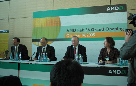
A little under 6 months ago AMD introduced their first 300mm 90nm manufacturing facility, called Fab 36. The name of course comes from its existence 36 years after the founding of AMD, with the plant itself being located next to Fab 30 in Dresden, Germany.
The grand opening of Fab 36 was mostly for media attention as the plant would not begin shipping revenue parts until Q1 of 2006. That sometime is today as AMD has just announced that Fab 36 is finally shipping revenue parts. The parts that it is shipping are 90nm Athlon 64 and Sempron CPUs, so Opterons and Athlon 64 X2s will still come out of Fab 30 next door. AMD cites customer demand as the reason that Athlon 64 and Sempron are first out of the new fab, which honestly makes sense; there's always need for more capacity at the lower end.
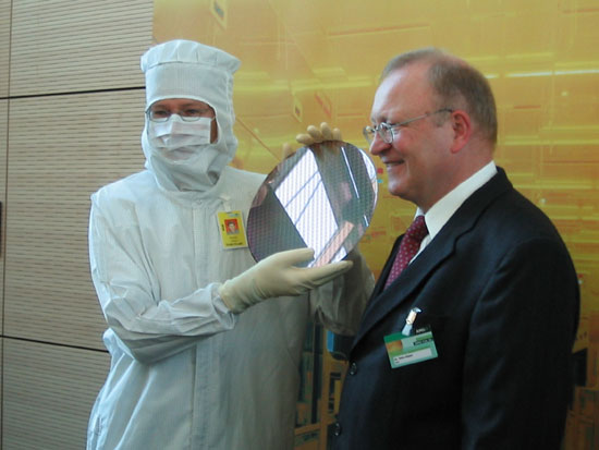
Although both Fab 30 and Fab 36 produce 90nm processors, Fab 30 uses smaller 200mm wafers while Fab 36 features an upgrade to 300mm wafers. AMD says that yields on 300mm wafers coming out of Fab 36 are comparable to 200mm yields being produced at Fab 30.
In terms of capacity, by 2008 AMD plans to be able to crank out 20,000 (300mm) wafers per month out of Fab 36 which would double its microprocessor production capacity to approximately 100M CPUs per year (thanks to larger wafers and smaller transistors). For comparison, Fab 30 currently produces 30,000 (200mm) wafers per month. Unfortunately AMD was unable to provide us with any sort of guidance as to how quickly Fab 36 will ramp up to its 20K per month target. AMD's partnership with Chartered Semiconductor Manufacturing Ltd. out of Singapore will guarantee additional 90nm production capacity beginning in the second half of this year. By the end of this year, AMD's capacity will have increased tremendously over the single fab they had producing 90nm parts previously.
As we mentioned in our initial coverage of Fab 36's grand opening, all parts shipping out of the plant will be 90nm, with AMD converting to 65nm starting in the second half of this year. Fab 36 will be "substantially converted" to 65nm manufacturing by the middle of 2007. Once again, AMD wasn't able to provide us with any sort of concrete details about the ramp to 65nm. It could very well be that AMD will be shipping lots of revenue generating 65nm parts by the end of this year, or they could be shipping very little. If the latter is true, then AMD's real transition to 65nm won't occur until far into 2007. When it does happen however, the move to 65nm will bring about smaller die sizes, faster switching transistors and lower power consumption for AMD, just as it has for Intel. AMD's 65nm process will incorporate their third generation of SOI technology to further reduce power consumption. AMD is promising a 40% increase in transistor performance with the move to 65nm thanks to the smaller process and the third generation SOI technology.
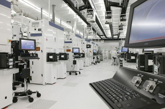
Fab 36 in Action


68 Comments
View All Comments
Viditor - Friday, April 7, 2006 - link
Of course it can...don't you read reviews?
If you read http://www.xbitlabs.com/articles/cpu/display/sempr...">this X-Bit review (granted there aren't a lot of reviews on Sempron), you'll see it runs neck and neck (and in many cases better) with the A64 3000+ which Anand directly compared to the 805 http://www.anandtech.com/cpuchipsets/showdoc.aspx?...">here.
As Anand said in his conclusion:
"Gamers looking for a temporary upgrade should honestly look to the Athlon 64 3000+ instead, as very few games have boarded the dual train as of now"..."if you are a multitasker or run multithreaded applications, and you want a great low cost solution, then the Pentium D 805 makes a wonderful stepping stone to a future AM2 or Conroe platform. If you're a gamer that doesn't care about multitasking while gaming, the Athlon 64 3000+ is still a strong value"
In addition, if you look at the power usage page of Anand's review, you'll note that the 805 requires a power plant of it's own...:) (j/k)
blackbrrd - Tuesday, April 4, 2006 - link
Bullshit ;)Anandtech was one of the first review sites to match the Opteron up vs the Xeon, which showed Opteron spanking Xeons. Haven't seen anything like those reviews from any other sites.
hans007 - Tuesday, April 4, 2006 - link
they have used a lot of vague terminology.i.e. our wafer yields at 300mm are equal to 200mm.
that means, what?
that they get the same number of cpus out of 300mm and 200mm. or the percenteage of the wafer yield?
they also have no 65nm demos at all even though they claim to be sampling the cpus. and they claim 40% better transistor performance, but that probably just means it say uses up less power not switching faster.
so it all depends on just the exact details of what that all means.
AnnonymousCoward - Saturday, April 8, 2006 - link
"Yield" refers to the percentage of good die.40% better transistor performance isn't merely talking about power. Performance means performance. It's also not saying the CPU is going to be 40% faster. There's propagation delays involved with transistor circuits, and some low level figure will be sped up by 40% (I don't know if it's rise/fall times, propagation delay, switching frequency, etc).
Calin - Wednesday, April 5, 2006 - link
As a 300mm wafer has more than twice the size of a 200mm wafer, they should produce twice as much processors from a 300mm wafer. Maybe more, as less space is lost on the sides.Anyway, why they don't make the wafers square? that would decrease the area lost on sides
stephenbrooks - Thursday, April 6, 2006 - link
I think they should make the chips round.Zoomer - Sunday, April 9, 2006 - link
That will be even worse, unless 1 chip == 1 wafer. And that's insane.eetnoyer - Wednesday, April 5, 2006 - link
I guess you don't know how wafers are made. The silicon is originally made sort of like homemade rock candy (Put a string tied to a pencil into a jar of hot, sugar-saturated water) and thus comes out in a columnar shape (I know, very rough analogy). After that, the wafers are made by taking slices off of the column. I suppose they could square the columns before slicing, but then there would be alot of waste, the cost of which would still be passed onto the chip maker. Much more efficient to just get that extra production out of the circular wafer.....it doesn't really cost any extra.Calin - Thursday, April 6, 2006 - link
No, I didn't knew. Thanks for the explanation.I remember I heard about diamond "wafers" that were made by growing a rectangular substrate - and once it was thick enough, they would cut it in several smaller slices. The result would be a "brick". I somehow assumed silicon would be the same
menting - Tuesday, April 4, 2006 - link
exactly what I was thinking.also, that's comparing the 300mm and 200mm wafers at 90nm process only, which isn't too much of a feat to accomplish.
when the 300mm goes to 65nm process, the yield (% die/waf) will definitely go down some, how much we probably will never know. it could go down enough that a 300mm wafer will initially produce only about the same or a little more number of dies per wafer than the 200mm at 90nm does.
Basically this announcement regarding yields isn't saying much except for the expected.