An AMD Update: Fab 36 Begins Shipments, Planning for 65nm and AM2 Performance
by Anand Lal Shimpi on April 4, 2006 11:00 AM EST- Posted in
- CPUs
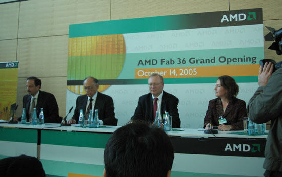
A little under 6 months ago AMD introduced their first 300mm 90nm manufacturing facility, called Fab 36. The name of course comes from its existence 36 years after the founding of AMD, with the plant itself being located next to Fab 30 in Dresden, Germany.
The grand opening of Fab 36 was mostly for media attention as the plant would not begin shipping revenue parts until Q1 of 2006. That sometime is today as AMD has just announced that Fab 36 is finally shipping revenue parts. The parts that it is shipping are 90nm Athlon 64 and Sempron CPUs, so Opterons and Athlon 64 X2s will still come out of Fab 30 next door. AMD cites customer demand as the reason that Athlon 64 and Sempron are first out of the new fab, which honestly makes sense; there's always need for more capacity at the lower end.
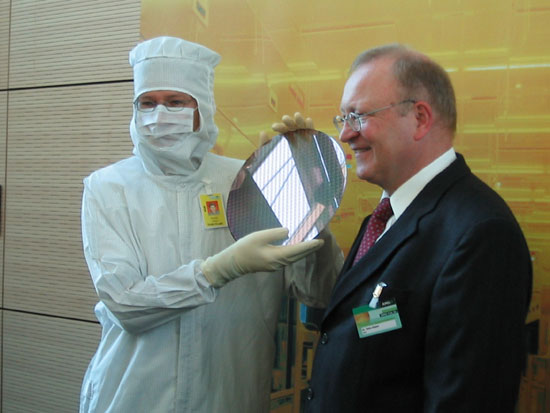
Although both Fab 30 and Fab 36 produce 90nm processors, Fab 30 uses smaller 200mm wafers while Fab 36 features an upgrade to 300mm wafers. AMD says that yields on 300mm wafers coming out of Fab 36 are comparable to 200mm yields being produced at Fab 30.
In terms of capacity, by 2008 AMD plans to be able to crank out 20,000 (300mm) wafers per month out of Fab 36 which would double its microprocessor production capacity to approximately 100M CPUs per year (thanks to larger wafers and smaller transistors). For comparison, Fab 30 currently produces 30,000 (200mm) wafers per month. Unfortunately AMD was unable to provide us with any sort of guidance as to how quickly Fab 36 will ramp up to its 20K per month target. AMD's partnership with Chartered Semiconductor Manufacturing Ltd. out of Singapore will guarantee additional 90nm production capacity beginning in the second half of this year. By the end of this year, AMD's capacity will have increased tremendously over the single fab they had producing 90nm parts previously.
As we mentioned in our initial coverage of Fab 36's grand opening, all parts shipping out of the plant will be 90nm, with AMD converting to 65nm starting in the second half of this year. Fab 36 will be "substantially converted" to 65nm manufacturing by the middle of 2007. Once again, AMD wasn't able to provide us with any sort of concrete details about the ramp to 65nm. It could very well be that AMD will be shipping lots of revenue generating 65nm parts by the end of this year, or they could be shipping very little. If the latter is true, then AMD's real transition to 65nm won't occur until far into 2007. When it does happen however, the move to 65nm will bring about smaller die sizes, faster switching transistors and lower power consumption for AMD, just as it has for Intel. AMD's 65nm process will incorporate their third generation of SOI technology to further reduce power consumption. AMD is promising a 40% increase in transistor performance with the move to 65nm thanks to the smaller process and the third generation SOI technology.
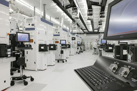
Fab 36 in Action


68 Comments
View All Comments
Homerr - Wednesday, April 5, 2006 - link
I keep looking but can't find when AM2 is supposed to be introduced. Can anyone enlighten me?Viditor - Wednesday, April 5, 2006 - link
6/6/06...
Toadster - Wednesday, April 5, 2006 - link
The grand opening of Fab 36 was mostly for media attention as the plant would not begin shipping revenue parts until Q1 of 2006. That sometime is today as AMD has just announced that Fab 36 is finally shipping revenue parts.Q1 ended last week LOL
hans007 - Wednesday, April 5, 2006 - link
i think a lot of it defeinitely is spin doctoring.another factor is that the dies are all single core dies which yield higher than dual core ones (since the dual core ones are not seperate like say presler if one of them is bad all of it is bad).
that said, the way amd make it sound it look slike their capacity will be greatly increased in the future because they can now make smallre chips. which is pretty stupid.
since even if they go to 65nm by the time 65nm is out everything intel makes will be dual core. so amd will have to sell everything dual core as well. so all the dies will be twice the size making the chips per wafer the same as it is now 90nm @ 300mm.
MrKaz - Wednesday, April 5, 2006 - link
That’s a good point.But this is only valid if Intel can get bad dual cores into single cores.
In the case of Presler, Intel for each 2 good chips get 1, so isn’t this the same of getting just one dual?
coldpower27 - Wednesday, April 5, 2006 - link
Yileding 2x 81mm2 dies is much easier then yielding AMDs single monolothic Toledo of 199mm2 or Windsor of 220mm2. If there is a defect in the processor core logic the Dual Core is completely useless and has to be thrown out. If it is the cache then they can make a lower cache Dual Core out of it.With Cedar Mill/Presler Intel is in a great position to address market needs as that core can be binned in 3 different SKU's.
Celeron D 35x Cedar Mill 512KB, disable part of the cache.
Pentium 4 6x1 Cedar Mill.
Pentium D Presler, 2 fully functioning Cedar Mill cores, from 2 different wafers even.
Viditor - Wednesday, April 5, 2006 - link
True...but it really hurts performance.
Honestly, if it was such an advantageous design financially then why would Intel design Conroe with a shared cache? I don't think the yields are affected as much as the spin doctors at Intel would have you believe...
coldpower27 - Wednesday, April 5, 2006 - link
It's not a big deal for Conroe or Allendale, those are 14x mm2 or 11x mm2 in die area, once you get back down to this level on 300mm wafers it's not too too bad.The NetBurst design had reached the end of it's life now, since it can't compete on performance effectively, it might as well rake in the advantage of reduced costs, good yeilds and flexibility. Since there isn't a ODMC, there isn't a reason to keep the dies together as NetBurst functions identically if the dies are seperate in Dual Core configuration.
The Dual Die implementation is an effective one, Intel will be using it for Kentsfield and Clovertown, on the 65nm process. Allowing them to put two Conroes or Woodcrests on a single MCM package. We'll see if it affects performance on Core Architecture negatively to the degree that it will uncompetitive. There is more then one way to extract performance.
Viditor - Wednesday, April 5, 2006 - link
So you're saying that once AMD gets to 65nm they will have better percentage yields because it will be a smaller die?
Can't say I agree here...
The only advantage to "joining" the dice (either through DCMA or shared cache) is cache coherency and avoiding the FSB.
Since Kentsfield will be for the desktop and Quad Core Opterons will be Socket F only, the one to watch will be Cloverton. Frankly it won't be the MCM as much as the lack of a P2P platform that will make Cloverton as ineffective as Paxville is...that said, if you look at the difference in core scaling on AMD vs Intel in the single to dual core market (or in this case DCMA vs MCM), you'll see exactly what I'm talking about.
coldpower27 - Thursday, April 6, 2006 - link
Like I said I am gonna wait and see on Clovertown, it might be an issue, though again it might not. Funny you choose the worst NetBurst Dual Core as your example..., I am just gonna wait till I see the results in the server market. Paxville has access to a much older platform however, so I don't really take results to be of much use.
No I don't think so, when AMD gets to 65nm, they won't beat Intel in the die size department, an optical shrink of Windsor to 65nm Brisbane, would be from 220mm2 to 132mm2. It would also depend if it's a straight shrink or if AMD adds more features and what not to their cores. I expect their yeilds to drop some from a mature 90nm SOI process, but total yield should be somewhat better.
I guess I should be more clear, the die sizes for Conroe/Allendale are fine as they are for Intel on a 65nm process that has been in production for at least 2Q.
How do you disagree again, as NetBurst doesn't have shared cache, not at the consumer level at least, so they communicate through the FSB anyway. Since the NetBurst design communicates through the FSB, the DUal Die implementation is fine...