Cadence Delivers Technical Details on GDDR7: 36 Gbps with PAM3 Encoding
by Anton Shilov on March 8, 2023 4:45 PM EST
When Samsung teased the ongoing development of GDDR7 memory last October, the company did not disclose any other technical details of the incoming specification. But Cadence recently introduced the industry's first verification solution for GDDR7 memory, and in the process has revealed a fair bit of additional details about the technology. As it turns out, GDDR7 memory will use PAM3 as well as NRZ signaling and will support a number of other features, with a goal of hitting data rates as high as 36 Gbps per pin.
A Short GDDR History Lesson
At a high level, the evolution of GDDR memory in the recent years has been rather straightforward: newer memory iterations boosted signaling rates, increased burst sizes to keep up with those signaling rates, and improved channel utilization. But none of this substantially increased the internal clocks of the memory cells. For example, GDDR5X and then GDDR6 increased their burst size to 16 bytes, and then switched to dual-channel 32-byte access granularity. While not without its challenges in each generation of technology, ultimately the industry players have been able to crank up the frequency of the memory bus with each version of GDDR to keep the performance increases coming.

But even "simple" frequency increases are increasingly becoming not so simple. And this has driven the industry to look at solutions other than cranking up the clocks.
With GDDR6X, Micron and NVIDIA replaced traditional non-return-to-zero (NRZ/PAM2) encoding with four-level pulse amplitude modulation (PAM4) encoding. PAM4 increases the effective data transmission rate to two data bits per cycle using four signal levels, thus enabling higher data transfer rates. In practice, because GDDR6X has a burst length of 8 bytes (BL8) when it operates in PAM4 mode, it is not faster than GDDR6 at the same data rate (or rather, signaling rate), but rather is designed to be able to reach higher data rates than what GDDR6 can easily accomplish.
Four-level pulse amplitude modulation has an advantage over NRZ when it comes to signal loss. Since PAM4 requires half the baud rate of NRZ signaling for a given data rate, the signal losses incurred are significantly reduced. As higher frequency signals degrade more quickly as they travel through a wire/trace - and memory traces are relatively long distances by digital logic standards - being able to operate at what's essentially a lower frequency bus makes some of the engineering and trace routing easier, ultimately enabling higher data rates.
The trade-off is that PAM4 signaling in general is more sensitive to random and induced noise; in exchange for a lower frequency signal, you have to be able to correctly identify twice as many states. In practice, this leads to a higher bit error rate at a given frequency. To reduce BER, equalization at the Rx end and pre-compensation at the Tx end have to be implemented, which increases power consumption. And while it's not used in GDDR6X memory, at higher frequencies (e.g. PCIe 6.0), forward-error correction (FEC) is a practical requirement as well.
And, of course, GDDR6X memory subsystems require an all-new memory controllers, as well as a brand-new physical interface (PHY) both for processors and memory chips. These complex implementations are to a large degree the main reasons why four-level coding has, until very recently, been almost exclusively used for high-end datacenter networking, where the margins are there to support using such cutting-edge technology.
GDDR7: PAM3 Encoding for Up to 36 Gbps/pin
Given the trade-offs mentioned above in going with either PAM4 signaling or NRZ signaling, it turns out that the JEDEC members behind the GDDR7 memory standard are instead taking something of a compromise position. Rather than using PAM4, GDDR7 memory is set to use PAM3 encoding for high-speed transmissions.
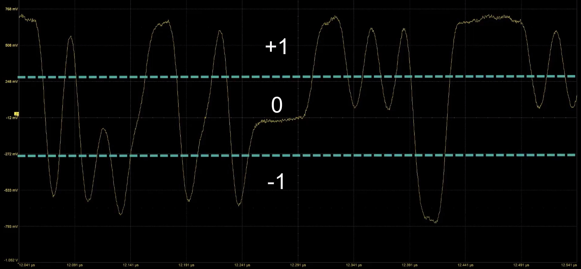
As the name suggests, PAM3 is something that sits between NRZ/PAM2 and PAM4, using three-level pulse amplitude modulation (-1, 0, +1) signaling, which allows it to transmit 1.5 bits per cycle (or rather 3 bits over two cycles). PAM3 offers higher data transmission rate per cycle than NRZ – reducing the need to move to higher memory bus frequencies and the signal loss challenges those entail – all the while requiring a laxer signal-to-noise ratio than PAM4. In general, GDDR7 promises higher performance than GDDR6 as well as lower power consumption and implementation costs than GDDR6X.
And for those keeping score, this is actually the second major consumer technology we've seen introduced that uses PAM3. USB4 v2 (aka 80Gbps USB) is also using PAM3 for similar technical reasons. To quote from our initial coverage back in 2021:
So what on earth in PAM3?
From Teledyne LeCroy on YouTube
PAM3 is a technology where the data line can carry either a -1, a 0, or a +1. What the system does is actually combine two PAM3 transmits into a 3-bit data signal, such as 000 is an -1 followed by a -1. This gets complex, so here is a table:
| PAM3 Encoding | ||
| AnandTech | Transmit 1 |
Transmit 2 |
| 000 | -1 | -1 |
| 001 | -1 | 0 |
| 010 | -1 | 1 |
| 011 | 0 | -1 |
| 100 | 0 | 1 |
| 101 | 1 | -1 |
| 110 | 1 | 0 |
| 111 | 1 | 1 |
| Unused | 0 | 0 |
When we compare NRZ to PAM3 and PAM4, we can see the rate of data transfer for PAM3 is in the middle of NRZ and PAM4. The reason why PAM3 is being used in this case is to achieve that higher bandwidth without the extra limitations that PAM4 requires to be enabled.
| NRZ vs PAM-3 vs PAM4 | |||
| AnandTech | Bits | Cycles | Bits Per Cycle |
| NRZ | 1 | 1 | 1 |
| PAM-3 | 3 | 2 | 1.5 |
| PAM-4 | 2 | 1 | 2 |
With that said,It remains to be seen how much power a 256-bit memory subsystem with the 36 Gbps data transfer rate promised by Samsung will use. The GDDR7 spec itself has yet to be ratified, and the hardware itself is still being constructed (which is where tools like Cadence's come in). But keeping in mind how bandwidth hungry applications for AI, HPC, and graphics are, that bandwidth will always be welcome.
Optimizing Efficiency and Power Consumption
In addition to increased throughput, GDDR7 is expected to feature a number of ways to optimize memory efficiency and power consumption. In particular, GDDR7 will support four different read clock (RCK) modes in a bid to enable it only when needed:
- Always running: Always running and stops during sleep modes;
- Disable: Stops running;
- Start with RCK Start command: Host can start RCK by issuing the RCK Start command before reading out dataand stop using the RCK Stop command when needed.
- Start with Read: RCK automatically starts running when DRAM receives any command which involves reading data out. It can be stopped using the RCK Stop command.
In addition, GDDR7 memory subsystems will be able to issue two independent commands in parallel. For example, Bank X can be refreshed by issuing a Refresh per bank command on CA[2:0], while Bank Y can be read by issuing a read command on CA[4:3] at the same time. Also, GDDR7 will support linear-feedback shift register (LFSR) data training mode to determine appropriate voltage levels and timings to ensure consistent data transfers. In this mode, the host will keep track of each individual eye (connection), which will allow it to apply appropriate voltages to better optimize power consumption.
Finally, GDDR7 will be able to shift between PAM3 encoding and NRZ encoding modes based on bandwidth needs. In high bandwidth scenarios, PAM3 will be used, while in low bandwidth scenarios the memory and memory controllers can shift down to more energy efficient NRZ.
Cadence Delivers First GDDR7 Verification Solution
While JEDEC has not formally published the GDDR7 specification, this latest technical data dump comes as Cadence has launched their verification solution for GDDR7 memory devices. Their solution fully supports PAM3 simulation by a real number representation, it supports binary bus, strength modeling, and real number modeling.
The verification IP also supports various modes of error injection in multiple fields of transactions during array data transfer and interface trainings. Furthermore, it comes with the waveform debugger solution to visualize transactions on the waveform viewers for faster debugging and verification.
"With the first-to-market availability of the Cadence GDDR7 VIP, early adopters can start working with the latest specification immediately, ensuring compliance with the standard and achieving the fastest path to IP and SoC verification closure," a statement by Cadence reads.
When Will GDDR7 Land?
While GDDR7 promises major performance increases without major increases of power consumption, perhaps the biggest question from technical audiences is when the new type of memory is set to become available. Absent a hard commitment from JEDEC, there isn't a specific timeframe to expect GDDR7 to be released. But given the work involved and the release of a verification system from Cadence, it would not be unreasonable to expect GDDR7 to enter the scene along with next generation of GPUs from AMD and NVIDIA. Keeping in mind that these two companies tend to introduce new GPU architectures in a roughly two-year cadence, that would mean we start seeing GDDR7 show up on devices later on in 2024.
Of course, given that there are so many AI and HPC companies working on bandwidth hungry products these days, it is possible that one or two of them release solutions relying on GDDR7 memory sooner. But mass adoption of GDDR7 will almost certainly coincide with the ramp of AMD's and NVIDIA's next-generation graphics boards.
Source: Cadence


29 Comments
View All Comments
Samus - Thursday, March 9, 2023 - link
It all comes down to architecture. AMD has seemed to historically favor a faster, wide memory bus, while nVidia has historically been less sensitive to the memory subsystem. Most AMD architectures are memory bandwidth starved while nVidia architectures are clock (effectively power\current) starved. GCN and Maxwell are two great examples of this; GCN-based Fiji cards brought HBM while Maxwell brought large L2 cache with a tremendously reduced memory bus, most cards having 128-bit, 192-bit, 224-bit or 256-bit opposed to AMD having a mainstream 256-bit to 384-bit, with 4096-bit at the high end.mode_13h - Thursday, March 9, 2023 - link
* I think you're over-generalizing. Don't try to fit trends, but rather look at it case-by-case.* Maxwell indeed went up to 384-bit, which it needed to counter Fury.
* Even then, Maxwell could only tie Fury by switching to tile-based rendering.
* Fury had 4096-bit, but the memory clock was just 1/6th of its GDDR5-based brethren.
* Vega only had 2048-bit, at a higher clock. Still, lower bandwidth than Fury.
* Vega 20 had 4096-bit, at an even higher clock, but didn't increase shaders or ROPs from Vega.
* Pascal further increased bandwidth efficiency by improving texture compression.
* RDNA 2 @ 256-bit was able to counter RTX 3000 @ 384-bit, by using Infinity Cache.
* RTX 4000 countered by increasing its L2 cache to comparable levels, will maintaining 384-bit.
Zoolook - Friday, March 17, 2023 - link
HBM was also less powerhungry, which AMD needed since their silicon was less efficient than Nvidias at that time, and it was an early bet on new technology, they were clearly betting on a more rapid uptake of HBM and lower future prices.HBM might have been a goner without AMDs bet on it which would have been a shame.
JasonMZW20 - Tuesday, March 14, 2023 - link
I think this just shows how much effort Nvidia put into delta color compression (DCC). By Pascal, Nvidia were able to compress a large majority of the screenspace, saving a ton of bandwidth in the process. AMD was also onboard the DCC train with Fiji/Tonga, and improved it again in Polaris. By Vega 10/Vega 20, it wasn’t external memory bandwidth holding these architectures back, rather registers and local caches at the CUs that were under increasing pressures, as well as poor overall geometry performance in graphics workloads. RDNA sought to fix those issues and did so.With the explosion of compute performance in high-end GPUs and also ray tracing, memory bandwidth is again a major limitation across the die, usually at the SM or CU level, as they expend registers and local caches processing ever larger datasets. Nvidia would not have dedicated so much die space to a very large 96MB L2 cache (full-die AD102 maximum) if it didn’t have significant benefits. Same for AMD in RDNA2 at 128MB L3 in Navi 21.
mode_13h - Wednesday, March 15, 2023 - link
> By Vega 10/Vega 20, it wasn’t external memory bandwidth holding these architectures backUm, the gains made by Vega 20 were primarily due to increasing memory bandwidth by more than 2x. That, and a clock speed bump. No microarchitecture changes, though.
But, Vega 20 was not made for gaming. Rather, it was destined for compute workloads, with a full contingent of fp64 and newly-added packed arithmetic instructions targeting AI.
> RDNA sought to fix those issues and did so.
Indeed, it significantly closed the gap between AMD GPUs' on-paper vs. real-world performance.
> With the explosion of compute performance in high-end GPUs and also
> ray tracing, memory bandwidth is again a major limitation across the die
If you just look at RDNA2 vs. RTX 3000, it seems pretty clear that AMD's outsized performance was largely thanks to Infinity Cache. Nvidia's resurgence in RTX 4000 suspiciously coincides with them adding massive amounts of L2 cache. These data points suggest that memory bandwidth is very much a live issue, even for raster performance.
Unfortunately, AMD took a step back on cache size in RDNA3. I hope we'll see a 3D V-Cache version of Navi 31 that steps it up to 192 MB or more. How nuts would it be if they even manage to reuse the very same V-Cache dies they're using in the Ryzen 7000X3D CPUs?
eSyr - Thursday, March 9, 2023 - link
PAM3 enables not 1.5, but rather log_2(3) bits per cycle (which can be rounded down to 1.5, but still); the fact that 1.5 equals to 3/2 might mislead the reader with regards to the way how information density is calculated.DanNeely - Thursday, March 9, 2023 - link
They're only using 8/9 possible symbols so 1.5 not 1.584... is the correct value. 0/0 isn't used presumably because they'd then need something else to indicate pathalogical data transmitted vs no signal.Silver5urfer - Thursday, March 9, 2023 - link
Now it makes sense. Why Nvidia top end GA102 cards (RTX3090Ti) and AD102 cards utilize ECC. In NVCP you can set the ECC on or off. HWbot started enforcing it for all the masses but for their own they allow it. As ECC enabling means less Memory performance, overall dragging the top scores. Ultimately PAM4 with such high clock / data rate = Errors / Noise so ECC was the solution that Nvidia implemented.G6X is really a beta test vehicle for all of Ampere. In fact entire Ampere lineup is a beta. MLCC reference shenanigans, then the Amazon game burning up cards, then the RTX3090 VRAM disaster which Nv says it's fine, Datasheets have 118C still it's way too high. Only card worth buying in Ampere is 3090Ti as they use 2Gb modules of Micron G6X and runs at full speed as intended without all this drama plus has ECC, and ofc it's not available anymore.
Moving along, I hope Samsung makes a comeback to Memory with GDDR7. Micron Memory is not really top end for GDDR. For NAND Flash Samsung is faltering bad (see - 980 Pro Firmware issues, 990 Pro NAND wear, and Micron high layer NAND has a lot more TBW, Firecuda 530).
A5 - Friday, March 10, 2023 - link
ECC is an optional feature that NV has available for error-sensitive compute applications. They generally recommend leaving it off (except on Gx100 products with HBM) as it incurs a 10% performance hit.