AMD Zen 4 Ryzen 9 7950X and Ryzen 5 7600X Review: Retaking The High-End
by Ryan Smith & Gavin Bonshor on September 26, 2022 9:00 AM ESTRyzen 7000 I/O Die: TSMC & Integrated Graphics at Last
We’ll start our look at the Ryzen 7000 silicon with the glue that holds the chip together: the I/O Die (IOD). Whether it’s a 7600X or 7950X – one CPU chiplet or two – every Ryzen 7000 processor gets one of AMD’s new IODs.
As with the Ryzen 3000/5000 series, the IOD is a die separate from the CPU core chiplets that hosts everything that isn’t the CPU cores or their associated L1/L2/L3 caches. By producing a 2 or 3 chiplet-based solution rather than a single monolithic die, AMD is able to put silicon that doesn’t require cutting-edge performance on a cheaper process node, while enjoying the yield advantages that come from smaller chiplets and older, more mature nodes.
And yet with that said, for the Ryzen 7000 series it’s AMD’s IOD that’s getting the biggest upgrade. Previously produced on GlobalFoundries’ 14nm/12nm process node, for Ryzen 7000 the IOD has made the leap to TSMC. The new IOD is made on TSMC’s 6nm process, a generation behind the 5nm node used for the CPU chiplets themselves, but a generation (and then-some) ahead of GlobalFoundries’ smallest node.
With AMD no longer tightly bound to GloFo with wafer share agreement exclusivity requirements, AMD is now free to produce chips like the IOD where they see fit. And with AMD also doing very well as a company in the last few years, they do not need to produce IODs at GloFo to meet their purchase requirements with the fab.
The jump to TSMC 6nm brings several advantages to AMD’s central chiplet. The much smaller process node allows for significantly more transistors – 3.4B on a 122m2 die, 63% more than before – which AMD can invest in new features such as integrated graphics. As well, the more efficient process node brings down the power requirements of the IOD, especially in near-idle situations, though AMD is relying on a lot more than process nodes here.
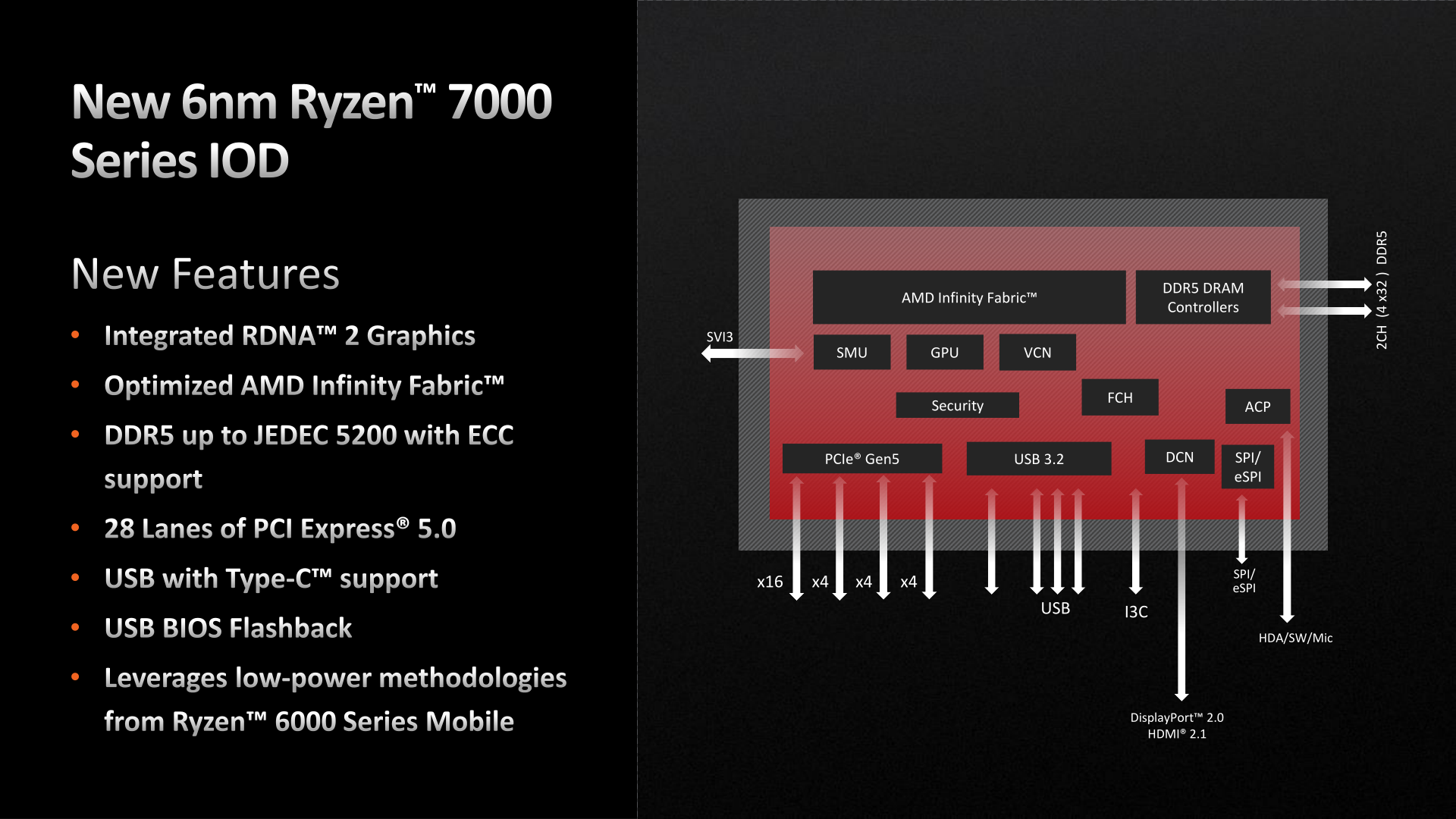
In terms of functionality, the IOD first and foremost is responsible for the CPU-side implementation of all the new features of the AM5 platform. So PCIe 5.0 root complexes, DDR5 memory support, updated display I/O, and more are implemented here. Relative to the Ryzen 3000/5000 IOD then, there is almost nothing here that AMD hasn’t touched in some function; even the USB controllers and infinity fabric have been altered for this generation of processors.
Ryzen 6000 Mobile’s Legacy: Power Control and Pluton
Outside of the obvious gains from moving to a smaller process node, the Ryzen 7000 IOD has also given AMD a chance to implement everything they’ve learned in the past 3 years about power control and power optimizations from the Ryzen mobile lineup. Since the previous-generation IOD was launched for the Ryzen 3000 family in 2019, AMD has launched the Ryzen 6000 Mobile CPU, a monolithic die design that went all-out on power efficiency improvements in a bid to catch up to Intel. Ryzen 6000 Mobile introduced power features such as SVI3, which have since been ported to the Ryzen 7000 design, and principally show up as parts of the IOD.
This was especially easy for AMD as the IOD is made on the same 6nm process as the Ryzen 6000 Mobile chips. Which means that the new IOD has been able to implement many of the same power gating, power binning, deep sleep modes, clock gating, and power state features that were first introduced for mobile. Which is to say that AMD has put a lot of hard work into keeping the IOD from working hard.
The Ryzen 7000 also inherits many of the basic security features of the Ryzen 6000 Mobile platform. AMD is still using their own Arm-based security processor within the IOD. And the new chip is compliant with Microsoft’s Pluton initiative as well – with all the mixed responses that will undoubtedly come from that.
Ryzen 7000 Becomes Whole: Integrated Graphics At Last
Of the additional 1.31B transistors in AMD’s new IOD, the single biggest spend against that budget comes from the long-awaited inclusion of integrated graphics on high-end Ryzen desktop parts. Up to this point, AMD’s high-end consumer Ryzen processors have not included integrated graphics; both the early monolithic parts and later chiplet-style parts have forgone them for cost and integration reasons. But now with AMD’s modern RDNA 2 graphics architecture and TSMC fabrication process, AMD has finally seen the (ray traced) light, and is building a small GPU block into the IOD to offer integrated graphics throughout the Ryzen 7000 product stack.
To be sure, this iGPU is not a very powerful one – and it’s not meant to be. With just 2 CUs (technically a single RDNA 2 dual compute unit), it offers one-sixth the number of CUs on AMD’s top-end Ryzen Mobile APUs, or in the bottom-of-the-stack discrete Radeon RX 6400. So this is not a configuration meant to replace AMD’s traditional APUs in laptop or desktop scenarios. None the less, it is a full implementation of the RDNA 2 architecture – ray tracing and all – in a very low performance configuration.
| AMD GPU Specificaiton Comparison | |||||
| AMD Radeon Graphics (Raphael) |
AMD Radeon 680M (Rembrandt) |
AMD Radeon RX 6400 | |||
| Stream Processors | 128 (2 CUs) |
768 (12 CUs) |
768 (12 CUs) |
||
| Boost Clock | 2200MHz | 2400MHz | 2321MHz | ||
| Peak Throughput (FP32) | 0.56 TFLOPS | 3.7 TFLOPS | 3.6 TFLOPS | ||
| Memory Clock | DDR5-5200 | LPDDR5-6400 | 16 Gbps GDDR6 | ||
| Memory Bus Width | 128-bit | 128-bit | 64-bit | ||
| Infinity Cache | N/A | N/A | 16MB | ||
| Manufacturing Process | TSMC N6 | TSMC N6 | TSMC N6 | ||
| Transistor Count | N/A | N/A | 5.4B | ||
| Architecture | RDNA2 | RDNA2 | RDNA2 | ||
| GPU | Raphael Integrated | Rembrandt Integrated | Navi 24 | ||
The idea behind including an iGPU here is to offer a basic implementation of modern graphics across the entire Ryzen 7000 lineup. Even though it’s not very fast, 2 CUs running at up to 2.2GHz is going to be fast enough for desktop work – and maybe even some very light gaming. This makes the high-end Ryzen chips suitable for desktop work and inclusion in OEM desktop systems without a discrete GPU, a market segment that AMD was previously locked out of and Intel enjoyed free reign. And even for users who are bringing their own GPU, an integrated GPU makes troubleshooting all the easier, as now it doesn’t require a separate video card to merely boot a system.
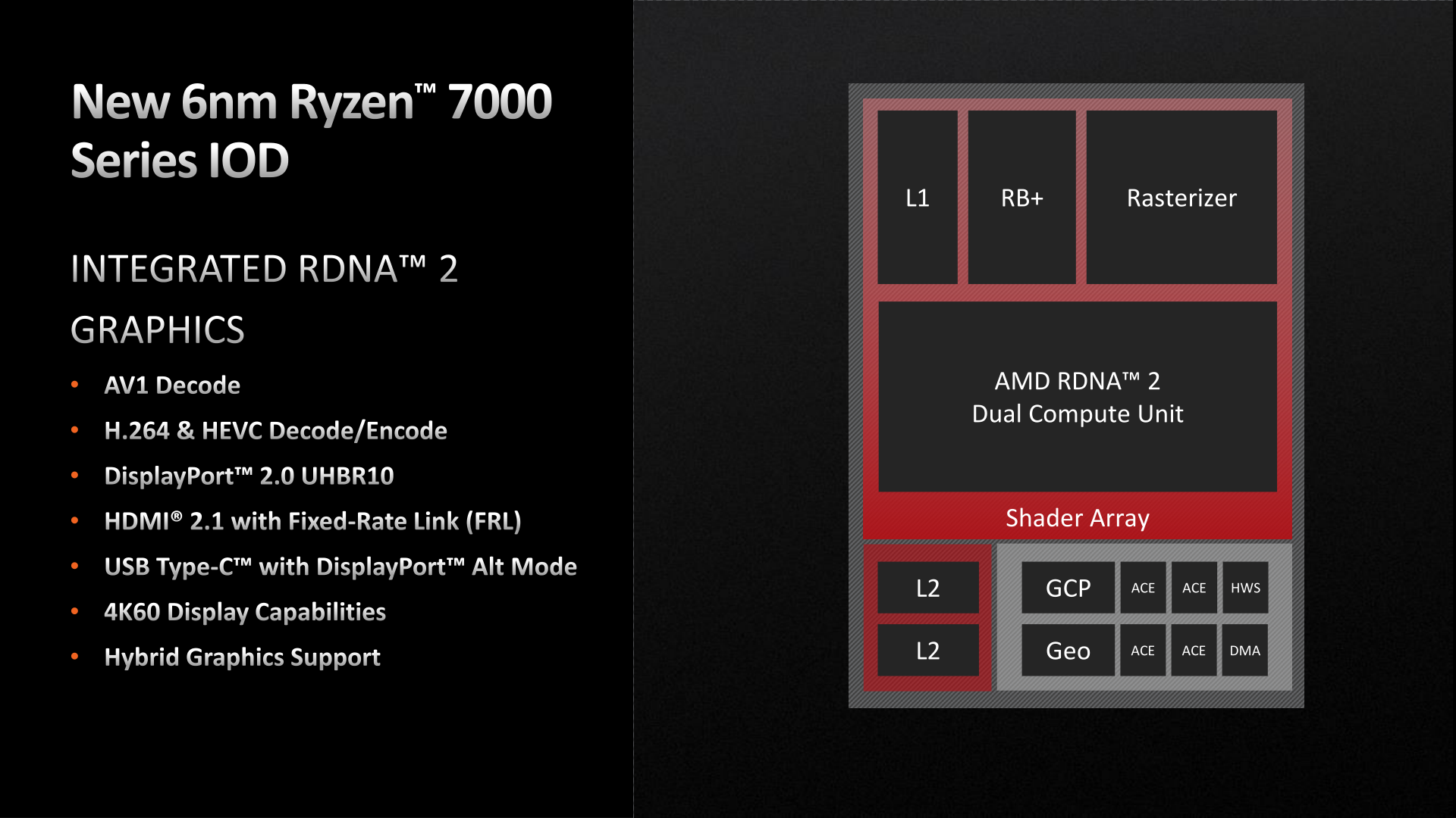
Besides enabling basic pixel processing, the other major function of the Ryzen 7000 iGPU is to enable all of the video decoding and video output functionality expected from a modern GPU. As this part is derived from the integrated GPU that when into Ryzen 6000 Mobile (Rembrandt), it comes with a very familiar feature set. That includes AV1, HEVC, and H.264 video decoding, as well as HEVC and H.264 video encoding. And, as AMD is keen to point out, these video encode/decode blocks remain accessible even with a discrete GPU in play; so unless a user outright disables the iGPU, every Ryzen 7000 system will have access to a modern suite of video encode and decode features.
Meanwhile on the display controller side of matters, this is the block that’s enabling Ryzen 7000 CPUs to drive up to 4 4K@60Hz displays. The iGPU display controllers can drive HDMI 2.1 up to its maximum 48Gbps data rate, or it can drive a DisplayPort 2.0 output at up to the UHBR10 data rate (a feature not even found on NVIDIA’s forthcoming RTX 40 series cards). And as mentioned previously when talking about motherboards and chipsets, motherboard vendors will have the option of exposing these DP outputs either via USB-C alt mode, or by implementing fixed DisplayPorts. All of which, in turn, can be used as active display outputs even if a discrete video card is installed, via AMD’s new hybrid graphics mode.
All told, AMD is taking a similar tack as Intel here with their desktop CPUs. Most (but not all) Intel desktop parts contain a basic UHD-class integrated Xe-LP GPU, which Intel does for many of the same reasons as AMD now is. AMD has a leg-up on Intel in as much as they offer a newer architecture and features to much, such as AV1 decoding. But we’ll have to see where performance lands; 2 Radeon CUs is low enough that these parts may not even catch up to Intel’s 32 EU integrated graphics.
AMD Infinity Fabric: Faster Flowing, Narrower Going
The last major functional update to come with AMD new IOD is the Infinity Fabric, AMD’s die-to-die interconnect. On the chiplet-based Ryzen desktop parts, IF is used to provide a low-latency connection between the IOD and the CPU core chiplet(s) on the package.
For the Ryzen 7000 series, AMD has done some further engineering work to reduce the power costs of the IF links, and thus improve the overall power efficiency of the link and reduce the data movement power penalty for using a chiplet-based approach. The most significant thing here is that AMD has doubled the IF link frequency, but cut the physical width of the IF link in half. As a result, Ryzen 7000’s IF links offer the same bandwidth as on Ryzen 5000,
According to AMD, this refactoring is because AMD’s engineers found that, contrary to conventional wisdom, they could save power running a narrower IF link at a higher frequency. Which is to say that, even though higher frequencies are normally power prohibitive, in the case of IF it’s just powering the physical links themselves which is the most expensive part. Part of that shift, in turn, comes from the fact that the newer process nodes have allowed AMD to run the IF link at a lower voltage,
Finally, further reducing AMD’s power consumption here, the IF links on the Ryzen 7000 now support multiple power states, versus the binary on/off states of the IF links on Ryzen 5000 and earlier. This gives AMD a nice middle ground to save power in lighter load situations, by being able to use intermediate states rather than running at full-power just to have an IF link active.
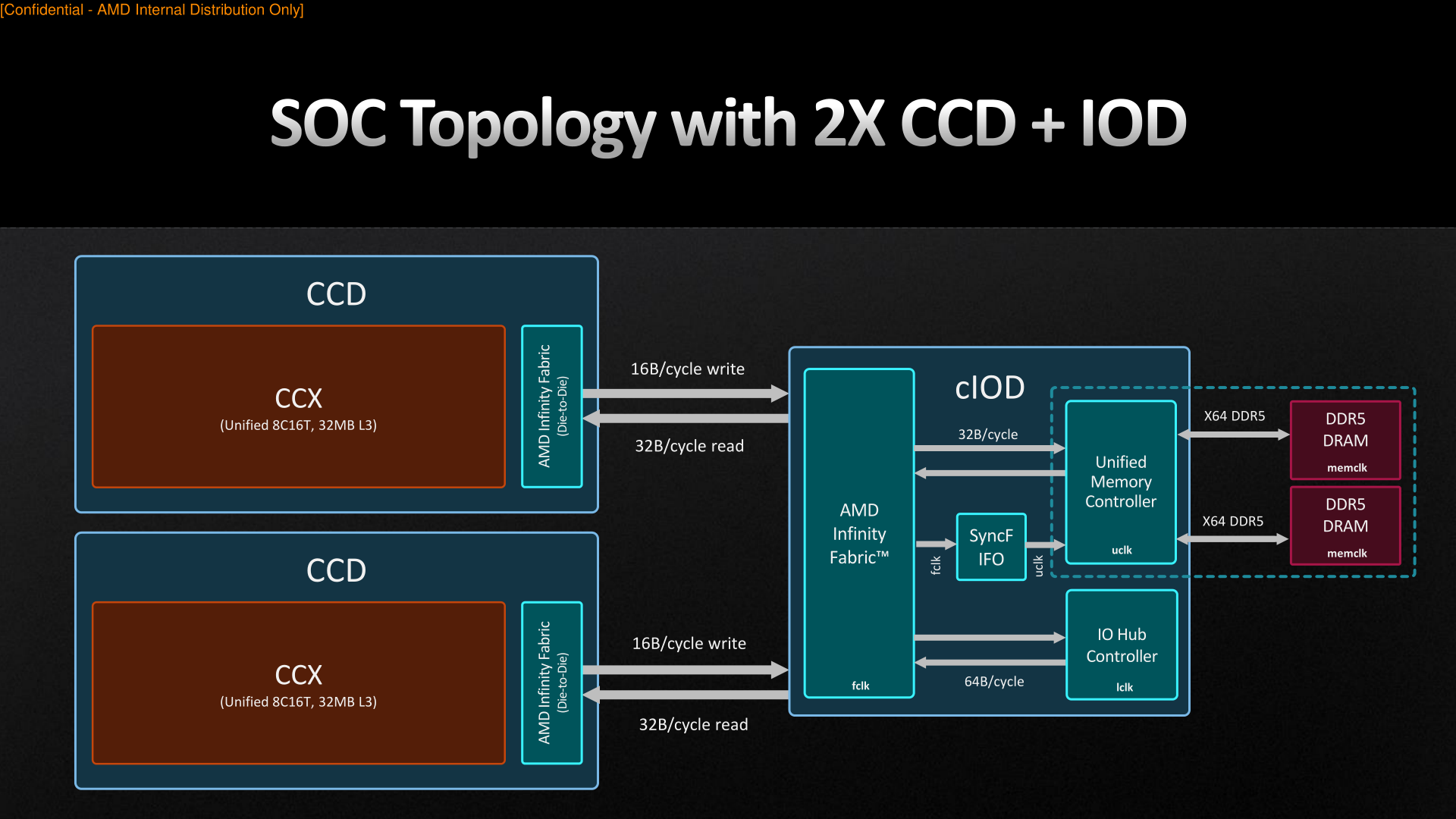
And while this leaves AMD with an obvious (if more power-hungry) route to take for more IF bandwidth in the future should they need it, for now the company intends to stay pat. According to AMD’s engineers, the amount of bandwidth supplied by the Ryzen 7000 IF links, though virtually identical to the amount of bandwidth on the Ryzen 5000 links, is still enough to meet AMD’s die-to-die bandwidth needs – even with extra memory bandwidth afforded by the switch to DDR5.


205 Comments
View All Comments
RomanPixel - Tuesday, September 27, 2022 - link
Me too! Replykmalyugin - Monday, September 26, 2022 - link
Wow, this article is almost unreadable. Was spellchecker turned off? Replyjonkullberg - Monday, September 26, 2022 - link
Gaming benchmarks with DDR5-6000 CL30 please! ReplyBushLin - Monday, September 26, 2022 - link
Exactly Replyxol - Monday, September 26, 2022 - link
wtf am I reading (context a part with tdp up to 170W from 105W) :"This has been possible through superior power efficiency, as Zencally a Zen 3 refinement, but on the new TSMC 5 nm process node (from TSMC 7 nm). This efficiency has allowed AMD to increase the overall TDP to 170 W from the previous 105 W but without too much penalty."
I can't even .. "too much penalty" ??
.. Looks like Zen has reached the end of the road imo (it had a good run) - none of the improvements here are from AMD - new DDR5, new 5nm node. The rest is "increase clocks/tdp" just like when Intel was stuck on 14nm.
I just don't know where they are going from here Reply
Threska - Monday, September 26, 2022 - link
Well we have " While Ryzen 7000 can drive a 2 DPC/4 DIMM setup, you’re going to lose 31% of your memory bandwidth if you go that route. So for peak performance, it’ll be best to treat Ryzen 7000 as a 1 DPC platform." and " Unfortunately, the compatibility situation is essentially unchanged from the AM4 platform, which is to say that while the CPU supports ECC memory, it’s going to be up to motherboard manufacturers to properly validate it against their boards.". The memory situation seems like a sticking point for a good while till things mature. ReplyBushLin - Monday, September 26, 2022 - link
Did you read the article? Put it in eco mode (105W for a 170W part) and it still stomps over everything in MT performance. Zen 4 is more about platform improvements, Zen 5 will be the microarchitecture overhaul. ReplyBushLin - Monday, September 26, 2022 - link
Stomping everything at 65W even! Replyxol - Tuesday, September 27, 2022 - link
Impressed that it's nominally $100 cheaper than a 5950X .Got to admit that. Replyxol - Tuesday, September 27, 2022 - link
Eco mode does perform better eg cinebench- b maybe +23% compared to 5950X, but it's using DDR5 5200 vs DDR4-3200 (?), and the power advantage can be assumed to come from 5nmMy original point still stands for me- 90% of benefits are from node and memory and allowing clocks as high as Tjunction allows - I don't think that is a great showing for AMD Reply