The Intel 12th Gen Core i9-12900K Review: Hybrid Performance Brings Hybrid Complexity
by Dr. Ian Cutress & Andrei Frumusanu on November 4, 2021 9:00 AM ESTCPU Tests: SPEC MT Performance - P and E-Core Scaling
Update Nov 6th:
We’ve finished our MT breakdown for the platform, investigating the various combination of cores and memory configurations for Alder Lake and the i9-12900K. We're posting the detailed scores for the DDR5 results, following up the aggregate results for DDR4 as well.
The results here solely cover the i9-12900K and various combinations of MT performance, such as 8 E-cores, 8 P-cores with 1T as well as 2T, and the full 24T 8P2T+8E scenario. The results here were done on Linux due to easier way to set affinities to the various cores, and they’re not completely comparable to the WSL results on the previous page, however should be within small margins of error for most tests.
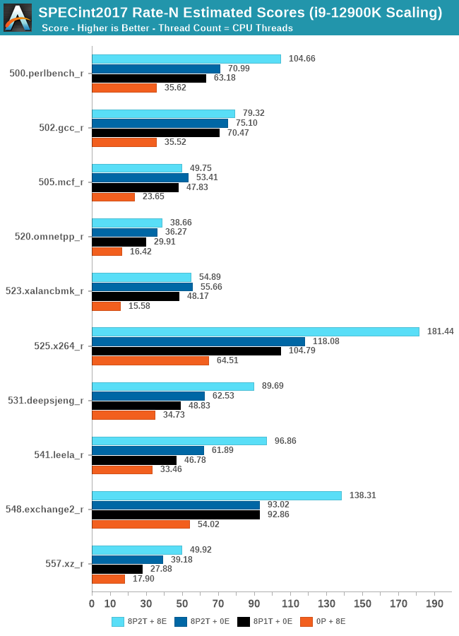
In the integer suite, the E-cores are quite powerful, reaching scores of around 50% of the 8P2T results, or more.
Many of the more core-bound workloads appear to very much enjoy just having more cores added to the suite, and these are also the workloads that have the largest gains in terms of gaining performance when we add 8 E-cores on top of the 8P2T results.
Workloads that are more cache-heavy, or rely on memory bandwidth, both shared resources on the chip, don’t scale too well at the top-end of things when adding the 8 E-cores. Most surprising to me was the 502.gcc_r result which barely saw any improvement with the added 8 E-cores.
More memory-bound workloads such as 520.omnetpp or 505.mcf are not surprising to see them not scale with the added E-cores – mcf even seeing a performance regression as the added cores mean more memory contention on the L3 and memory controllers.
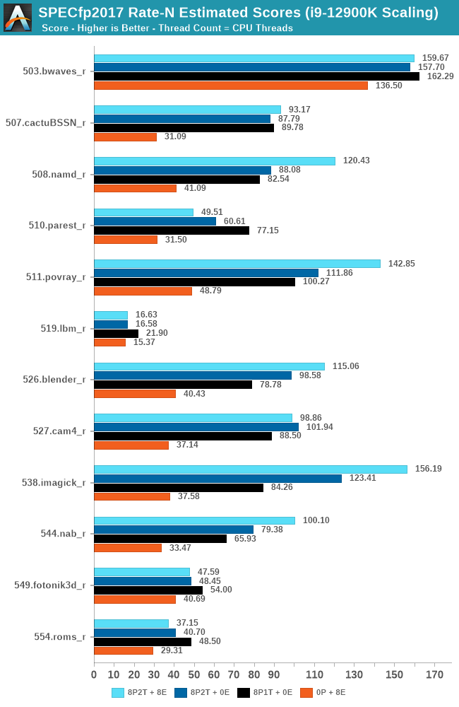
In the FP suite, the E-cores more clearly showcase a lower % of performance relative to the P-cores, and this makes sense given their design. Only few more compute-bound tests, such as 508.namd, 511.povray, or 538.imagick see larger contributions of the E-cores when they’re added in on top of the P-cores.
The FP suite also has a lot more memory-hungry workload. When it comes to DRAM bandwidth, having either E-cores or P-cores doesn’t matter much for the workload, as it’s the memory which is bottlenecked. Here, the E-cores are able to achieve extremely large performance figures compared to the P-cores. 503.bwaves and 519.lbm for example are pure DRAM bandwidth limited, and using the E-cores in MT scenarios allows for similar performance to the P-cores, however at only 35-40W package power, versus 110-125W for the P-cores result set.
Some of these workloads also see regressions in performance when adding in more cores or threads, as it just means more memory traffic contention on the chip, such as seen in the 8P2T+8E, 8P2T regressions over the 8P1T results.
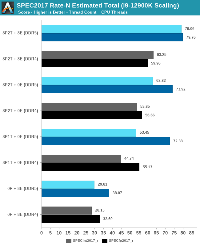
What’s most interesting here is the scaling of performance and the attribution between the P-cores and the E-cores. Focusing on the DDR5 set, the 8 E-cores are able to provide around 52-55% of the performance of 8 P-cores without SMT, and 47-51% of the P-cores with SMT. At first glance this could be argued that the 8P+8E setup can be somewhat similar to a 12P setup in MT performance, however the combined performance of both clusters only raises the MT scores by respectively 25% in the integer suite, and 5% in the FP suite, as we are hitting near package power limits with just 8P2T, and there’s diminishing returns on performance given the shared L3. What the E-cores do seem to allow the system is to allows to reduce every-day average power usage and increase the efficiency of the socket, as less P-cores need to be active at any one time.


474 Comments
View All Comments
mode_13h - Sunday, November 7, 2021 - link
I'm not even going to say this is a bad idea. The problem is that it's a big change and Intel normally prepares the software developer community for big new ISA extensions a year+ in advance!Again, what you're talking about is an ABI change, which is a big deal. Not only that, but to require code to handle dynamically switching between AVX2 and AVX-512 paths means that it can't use different datastructures for each codepath. It even breaks the task pre-emption model, since there need to be some limitations on where the code needs to have all its 512-bit registers flushed so it can handle switching to the AVX2 codepath (or vice versa).
This adds a lot of complexity to the software, and places a greater testing burden on software developers. All for (so far) one CPU. It just seems a bit much, and I'm sure a lot of software companies would just decide not to touch AVX-512 until things settle down.
GeoffreyA - Sunday, November 7, 2021 - link
My view on this topic is that Intel made a sound decision disabling AVX512. Some of the comments are framing it as if they made a mistake, because the tech community discovered it was still there, but I don't see any problem. Only, the wording was at fault, this controversial "fused off" statement. And actually, the board makers are at fault, too, enabling a hidden feature and causing more confusion.On the question of whether it's desirable, allowing one core with the instructions and another without, would've been a recipe for disaster---and that, too, for heaven knows what gain. The simplest approach was bringing both cores onto the same footing. Indeed, I think this whole P/E paradigm is worthless, adding complexity for minimal gain.
Oxford Guy - Monday, November 8, 2021 - link
‘Intel made a sound decision disabling AVX512’That’s not what happened.
O-o-o-O - Sunday, November 7, 2021 - link
Really? Our tech guys tried out Xeon Phi but couldn't make use of it. Years later, Xeon Phi was abruptly discontinued due to lack of demand. GPGPUs are much easier to handle.Yeah, coding cost and risks aside, it's interesting to see complex work of art in the modern CPU. But I'd rather wish for expansion of GPU support (like shared memory and higher band-width).
kwohlt - Sunday, November 7, 2021 - link
My understanding is that Raptor Lake's change is replacing Golden Cover P cores with Raptor Cove P cores, doubling Gracemont E-Cores per SKU, and using the same Intel 7 process. Granted, it's all leaks at this point, but with Gracemont being reused for Raptor Lake, I don't expect AVX-512 next year either.mode_13h - Monday, November 8, 2021 - link
> Raptor Lake's change is ... doubling Gracemont E-Cores ... using the same Intel 7 process.I was merely speculating that this *might* just be a transient problem. If they're using the same process node for Raptor Lake, which seems very plausible, then it's understandable if they don't want to increase the size or complexity of their E-cores.
However, there's some precedent, in the form of Knights Landing, where Intel bolted on dual AVX-512 pipelines + SMT4 to a Silvermont Atom core. And with a more mature Intel 7 node, perhaps the yield will support the additional area needed for just a single pipe + 512-bit registers. And let's not forget how Intel increased the width of Goldmont, yet simply referred to it as Goldmont+.
So, maybe Raptor Lake will use Gracemont+ cores that are augmented with AVX-512. We can hope.
GURU7OF9 - Saturday, November 6, 2021 - link
The is by far the best review I have read so far.A great comparison I would love to see just out of curiouslty would be to see P core only benchmarks and then e core only benchmarks! We could gain a much better understanding of the capabilities and performance of both .
This would bring a little bit of familiarity back to benchmarking .
nunya112 - Saturday, November 6, 2021 - link
the only info provided was its on intels new process 7 node. what does that mean? are they using TSMC and at 7nm? or did they finally crack 7nm at Intel?mode_13h - Sunday, November 7, 2021 - link
"Intel 7" is the process node formerly known as "10 nm ESF" (Enhanced SuperFin), which is the 4th generation 10 nm process, counting by the revisions they've introduced between the different products based on it. They like to pretend that Cannon Lake didn't happen, but that's why Ice Lake was actually 10 nm+ (2nd gen).They rebranded 10 nm ESF as "Intel 7" for marketing reasons, as explained here:
https://www.anandtech.com/show/16823/intel-acceler...
Hossein - Sunday, November 7, 2021 - link
It's funny that most reviewers are conveniently silent about the fact that there are quite a 'few' games which are incompatible AL.