Intel 12th Gen Core Alder Lake for Desktops: Top SKUs Only, Coming November 4th
by Dr. Ian Cutress on October 27, 2021 12:00 PM EST- Posted in
- CPUs
- Intel
- DDR4
- DDR5
- PCIe 5.0
- Alder Lake
- Intel 7
- 12th Gen Core
- Z690
Memory: Varies with Number of Modules
Inside each of the Alder Lake processors are memory controllers for both DDR5 and DDR4. Unlike previous generations, we’re unlikely to see motherboards supporting both types of memory. We understand that Intel has explicitly requested this – we didn’t see many retail combo boards in the DDR3/DDR4 era, so expect to see fewer this time around (although you can imagine someone will eventually do it). There is a slight technical reason too – DDR5 uses onboard power management, while DDR4 requires that from the motherboard, something which is hard to implement without wholly independent traces for both. If Intel is saying both cannot be done at the same time, then it’s likely that this is a unified DDR4+DDR5 controller that shares an amount of logic internally, but only one can be used at any one time.
Intel lists the specifications for its memory support as DDR4-3200 and DDR5-4800, and as always memory support is listed as conforming to the JEDEC implementations. This means Intel qualifies DDR4-3200 CL22, and anything above that is technically overclocking the CPU – it’s actually hard to find consumer memory at this speed these days. For DDR5, there are actually three specifications here:
| DDR5 JEDEC Specifications | |||||||
| AnandTech | Data Rate MT/s |
CL |
Peak BW GB/s |
Latency (ns) |
|||
| DDR5-4800 | A | 4800 | 34 | 34 | 34 | 38.40 | 14.17 |
| B | 40 | 40 | 40 | 16.67 | |||
| C | 42 | 42 | 42 | 17.50 | |||
We clarified with Intel that the processor supports all three, with the top being DDR5-4800A CL34. This is despite Intel shipping DDR5-4800B CL40 with their press kits, but I digress.
The thing with memory support is that it usually quoted for a specific number of modules installed into the system. In this case, Intel is quoting these numbers using one module per channel (technically a 64-bit channel, but more on that later), meaning that these are the supported speeds when two memory modules are supported. The official supported speed changes if you have more memory, double-sided memory, or dual rank memory.
We’ve seen this before – server processors are notorious for having slower support when more memory modules are installed. It turns out the more bandwidth you need, the harder it is to keep that speed with higher capacity memory. It was only until Intel’s 11th Gen Core products that the memory design supported DDR4-3200 regardless of configuration, because sometimes that’s how long it takes to optimize a memory controller. For Alder Lake, DDR4-3200 is also supported in any configuration, but DDR5 changes depending on the memory.
Intel shared this table with us.
If the motherboard has two memory slots total, then the maximum support is DDR5-4800 in any configuration.
If the motherboard has four memory slots total, then the maximum support is DDR5-4400 when two slots are filled with any memory.
If all four memory slots are filled, single rank memory will support up to DDR5-4000.
If all four memory slots are filled, dual-rank memory will support up to DDR5-3600.
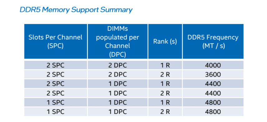
So technically Intel listing memory support on Alder Lake as DDR5-4800 is a bit of a misdirection compared to previous launches. If we were to look at parity, two modules in a four-slot board, then really we’d be quoting DDR5-4400. Funnily enough, all of Intel’s benchmarks presented at this launch were run at DDR5-4400, as per specification. Kudos to the testing team to staying within those guidelines.
A side note here on memory channels as a whole. In the desktop space, we’re used to one memory module having memory for one 64-bit memory channel. That’s true for DDR4, DDR3, DDR2 etc, but the DDR5 specifications move to 32-bit memory channels. So while each DDR5 module is still using 64-bits of bandwidth, there are technically two 32-bit memory channels worth of memory on each module. This can create a little bit of confusion, because it means that Intel 12th Gen, while still a 128-bit memory interface as previous generations, it uses 4x 32-bit channels, not 2x 64-bit. Undoubtedly companies (even Intel) still call this dual-channel, as a channel is usually inferred to be a 64-bit interface.
There is no easy solution here. 2DPC (two modules per channel) doesn’t really mean much if technically channel there infers 64-bit but you’re running on a 2x32-bit channel system. Some users are calling a DDR5 module a ’channel’ with two 32-bit ‘sub-channels’, although that is more a twisting of reality, given that sub-channels are often something else in memory design. Because we’ve used the word ‘module’ to imply a 64-bit channel for so long, and because memory can be installed with more than one module per 64-bit channel, it’s actually a mess in English to find not only the correct words but also ones simple enough to not make the situation overly complex. Perhaps it’s time for some new words.
Memory: XMP 3.0 and Better SPD
One of the new features with DDR5 is the expansion of Intel’s eXtreme Memory Profile support. Now moving to XMP 3.0, it increases flexibility for both users and vendors by increasing the number of profiles per module, opening up for customization, and improving the overclocking experience.
Memory vendors when they ship the memory will embed in the memory firmware a series of specifications, known as SPDs. For standard memory running to JEDEC specifications, the module will likely contain SPD profiles relating to something slow for underlying support, and then up to what the memory chips were sold at – depending on the motherboard, the system then picks the JEDEC SPD profile that best fits the processor (I’ve seen a wild variety of implementation here, funnily enough.
XMP goes above and beyond traditional SPD support.

XMP 2.0 on DDR4 contains up to two additional SPD profiles with overclocked values. For example, a DDR4-4000 CL16 memory module might have three profiles total – one at 2133 CL15, one at 3200 CL22, and a third XMP profile at 4000 CL16. It is up to the user to then select that profile when in the BIOS or through additional software. If the module has two XMP profiles, perhaps one for latency and another for bandwidth, then this can be done in XMP 2.0.
The update to XMP 3.0 allows for five profiles, rather than two. Three of these profiles are memory module vendor locked, limited by whatever they come out of the factory at. The final two profiles can be used by the memory module vendor, but are re-writable by users in order to save overclocking settings. These profiles can also be named to be descriptive.
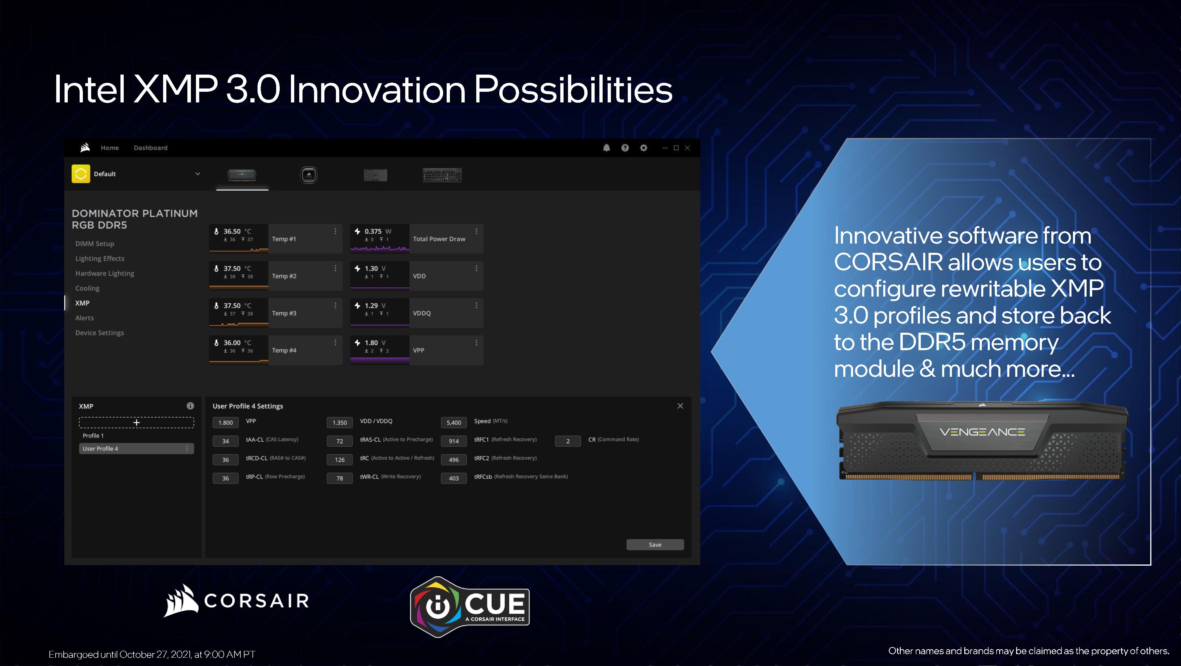
Intel states that this re-writing process is backed by a rigorous checksum support so users can’t brick their hardware. For most situations, that’s going to be reasonable, however if that security does get broken, it might be advised that if you buy second-hand DDR5 to erase those profiles and not use them. Just in case it overvolts the memory controller to 3 volts, or something.
Alongside more profiles, because DDR5 moves the power management for the module onto the module itself, if a memory vendor uses a ‘better than base’ solution then users can adjust various voltages and timings on a per-module basis.
Both the profile expansion and the updated voltage controls are also now exposed to the operating system in such a way that allows for better software implementation. Users with Corsair memory, for example, can use Corsair software to adjust the memory on the fly and monitor temperatures, power, voltages, and also keep track of how they fluctuate during overclocking, testing, or normal use. There is also another new feature, allowing users to adjust memory frequency on the fly, which has never been seen before. We’ll cover that in the next section.
On a more ecosystem level, we confirmed with Intel that XMP 3.0 is a self-certification procedure at memory vendors, with no additional licensing costs to the vendors.
Memory Gets Turbo: Dynamic Memory Boost
One of the persistent features with memory over the years is that when you have settings saved in the BIOS, they are ‘trained’ (tested to work) when the system boots up, and then that’s what you have for the whole time that the system is turned on. It never slows down, it never duty cycles to reduce power – it has been very consistent for a long time.
With Intel’s Z690 boards and 12th Gen Core Alder Lake processors, that changes. Much like processors and graphics have had idle states and turbo states for generations, memory now gets it as well.
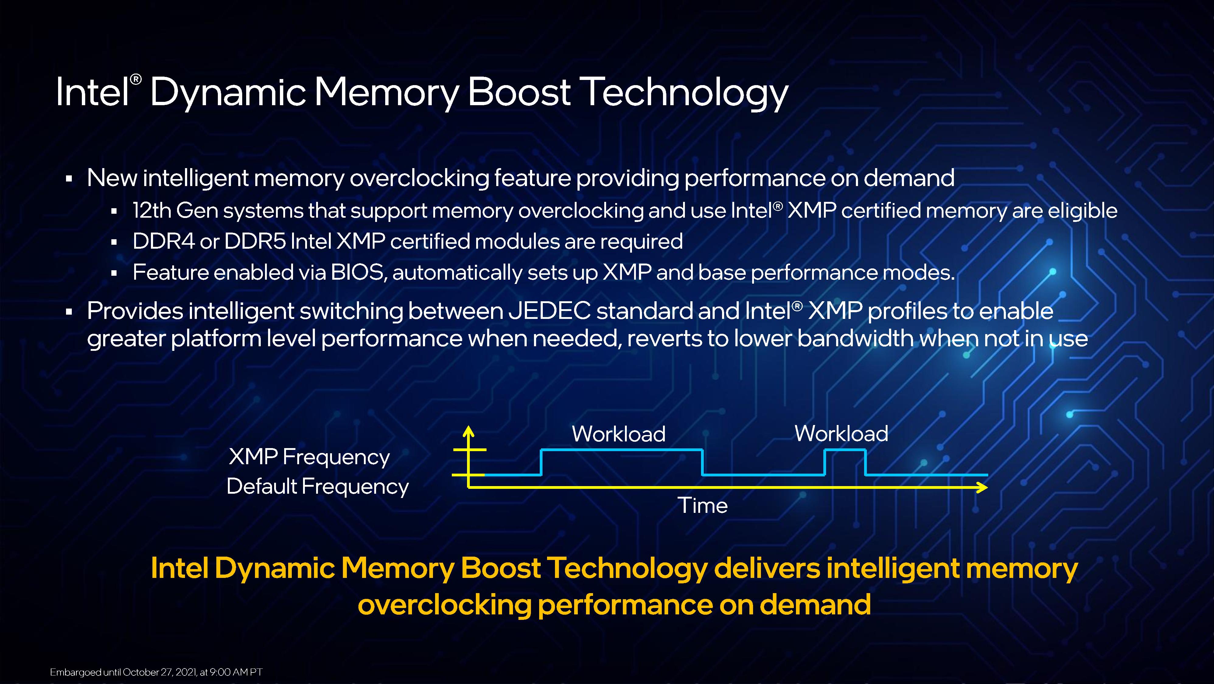
This first-generation technology is basic, but a start. A 12th Gen system, as long as it runs DDR4 or DDR5 memory with XMP, can define two of the onboard SPD profiles – one as the base, and one as the turbo. Usually the base profile is one of the immutable JEDEC profiles, and the turbo is an XMP profile. But when activated, the system is able to switch on the fly between the two, activating when a workload is initiated for higher performance, and supposedly better idle efficiency.
There are a few thoughts or questions on this worth noting:
#1: It works on DDR4? Intel says yes. This makes it sound like this is more of a software/firmware innovation than a hardware innovation, or it requires the right hardware on the CPU at least. No doubt if it works, it will become ubiquitous.
#2: Isn’t power efficiency really for benchmarks and laptops? I agree with this one, and expect it to be more of a highlighted feature when Alder Lake comes to laptops and notebooks. That being said, most notebook DRAM is JEDEC anyway, so it might open the doors for better-overclocked notebook memory if it can retain the battery life of a base JEDEC profile. Either that, or notebook memory will use a fast JEDEC profile in operation, then move to a more efficient but slower JEDEC profile on idle to save power.
#3: Doesn’t this introduce instability? Perhaps, but if it’s handled in the same way CPU turbo can be, then it shouldn’t be an issue.
In the same way we look to measure how CPU frequency ramps up from a performance request, we will have to look into tools to measure the same thing on memory, especially if more than a simple base/turbo system is developed for future use.


395 Comments
View All Comments
Bik - Saturday, October 30, 2021 - link
Let's check your argument. If 4 small cores > 1 big core while using same die area, how about just one big core for single thread performance and give us an addition of 24 more small cores? Clearly Intel (and Apple) not doing that, rather they reduce number of small cores (m1 pro, core i5 alderlake) instead. There clearly a catch, we'll know when review is out.Bik - Saturday, October 30, 2021 - link
7*4=28 cores. my math sucks.Wrs - Saturday, October 30, 2021 - link
For 1P 28E they'd probably run into fabric/coherency limits. If you have 30 nonlocking threads then that could be a rather efficient design. Let's see if we have that in a modern computer... *stares at the 10.5k CUDA cores on an RTX card*nandnandnand - Saturday, October 30, 2021 - link
Simple. You can have more than one task running at a time that can't be parallelized and will only respond to greater single-thread performance, and one or more applications running that can use multiple threads but not scale to benefit from dozens or hundreds of cores.Games will typically be using up to 8 cores in the upcoming generation because the PS5 and XSX have 8 cores and will be optimized to get the most out of 8. So Intel puts 8 big cores in the flagship but stops there. If the game can also use some of the small cores, great.
Also, we already know that next year's Raptor Lake will have up to 8 big cores and 16 small cores, and it looks like Intel will go to 8 big cores and 32 small cores after that. They can tweak to improve IPC across all the cores, but the small cores will be getting a greater proportion of the die area going foward. Apple has a different strategy, if their leaks are correct.
ThinkingReviewer200 - Friday, October 29, 2021 - link
Thanks for the article :)For the second page of the review, the sentence, "For performance, Intel lists a single P-core as ~19% better than a core in Rocket Lake 11th Gen" may have an inaccuracy. This percentage should perhaps be ~14% for according to the graph image 128% - 112% is 16% then 16%/112% is ~14% depending on the perspective, in this case perhaps the 11th gen. However, check this logic and math for these are percents inside percents calculations.
mode_13h - Saturday, October 30, 2021 - link
They're not additive. It's easier to see, if you drop the percentages and just call a Rocket Lake core 1.12x as fast as a Comet Lake core. Then, Alder Lake-P is 1.28x as fast as comet lake. So, Alder Lake-P should be 1.28/1.12 as fast as a Rocket Lake core which is 1.143 or about 14%.mode_13h - Saturday, October 30, 2021 - link
Ah, but if you look closely at the chart on page 2, it says "fixed-frequency". So, that's talking about essentially "instructions per clock". However, the stats on the last page are including clock speed differences.So, I guess that's how they get up to 19%? It would take only a clock speed increase of about 4.3% to makeup the difference. It's still not easy to see where they find that, but if both cores throttle back and Alder Lake's P core manages to hold a higher clock speed, then it's not hard to see how we could reach a 4.3% difference.
tech4fun - Friday, October 29, 2021 - link
I just canceled my Netflix account. Fanboi battle royale!nandnandnand - Friday, October 29, 2021 - link
What took you so long?Kendog52404 - Sunday, October 31, 2021 - link
Does Alder Lake support DDR4-3000 memory? Or, does it need to be 3200? I haven't bought memory for about 5 years, and it's DDR4-3000 that I had been planning to bring over from the old board. If I have to buy new memory, regardless, that changes things, and I'll need to take a serious look at DDR5.