Intel's Process Roadmap to 2025: with 4nm, 3nm, 20A and 18A?!
by Dr. Ian Cutress on July 26, 2021 5:00 PM ESTNew Technology Features for 2024: RibbonFETs
One of the major features of this roadmap is highlighted when it shifts to 20A, Intel’s process name referring to Angstroms rather than nanometers. At this juncture, as mentioned above, Intel will be transitioning from its FinFET design over to a new type of transistor, known as a Gate-All-Around transistor, or GAAFET. In Intel’s case, the marketing name they are giving their version is RibbonFET.
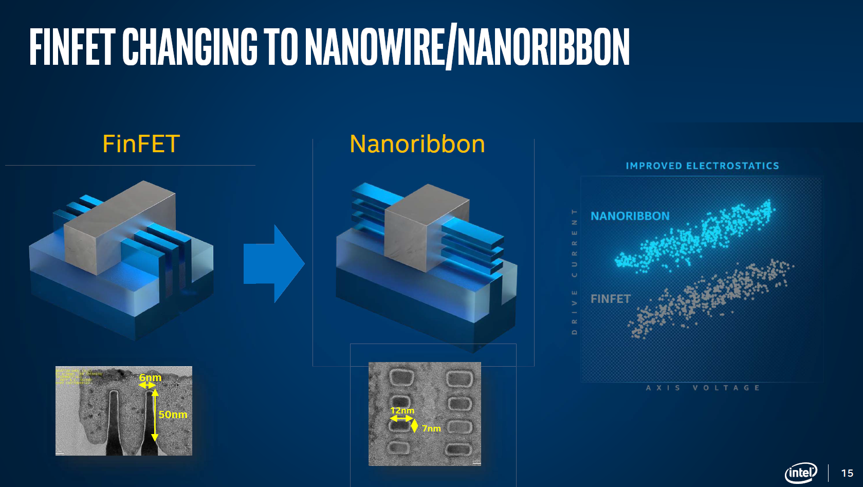
It has been widely expected that once the standard FinFET runs out of steam that the semiconductor manufacturing industry will pivot to GAAFET designs. Each of the leading edge vendors call their implementation something different (RibbonFET, MBCFET), but it is all using the same basic principle – a flexible width transistor with a number of layers helping drive transistor current. Where FinFETs relies on multiple quantized fins for source/drain and a cell height of multiple tracks of fins, GAAFETs enable a single fin of variable length, allowing the current for each individual cell device to be optimized in power, performance, or area.
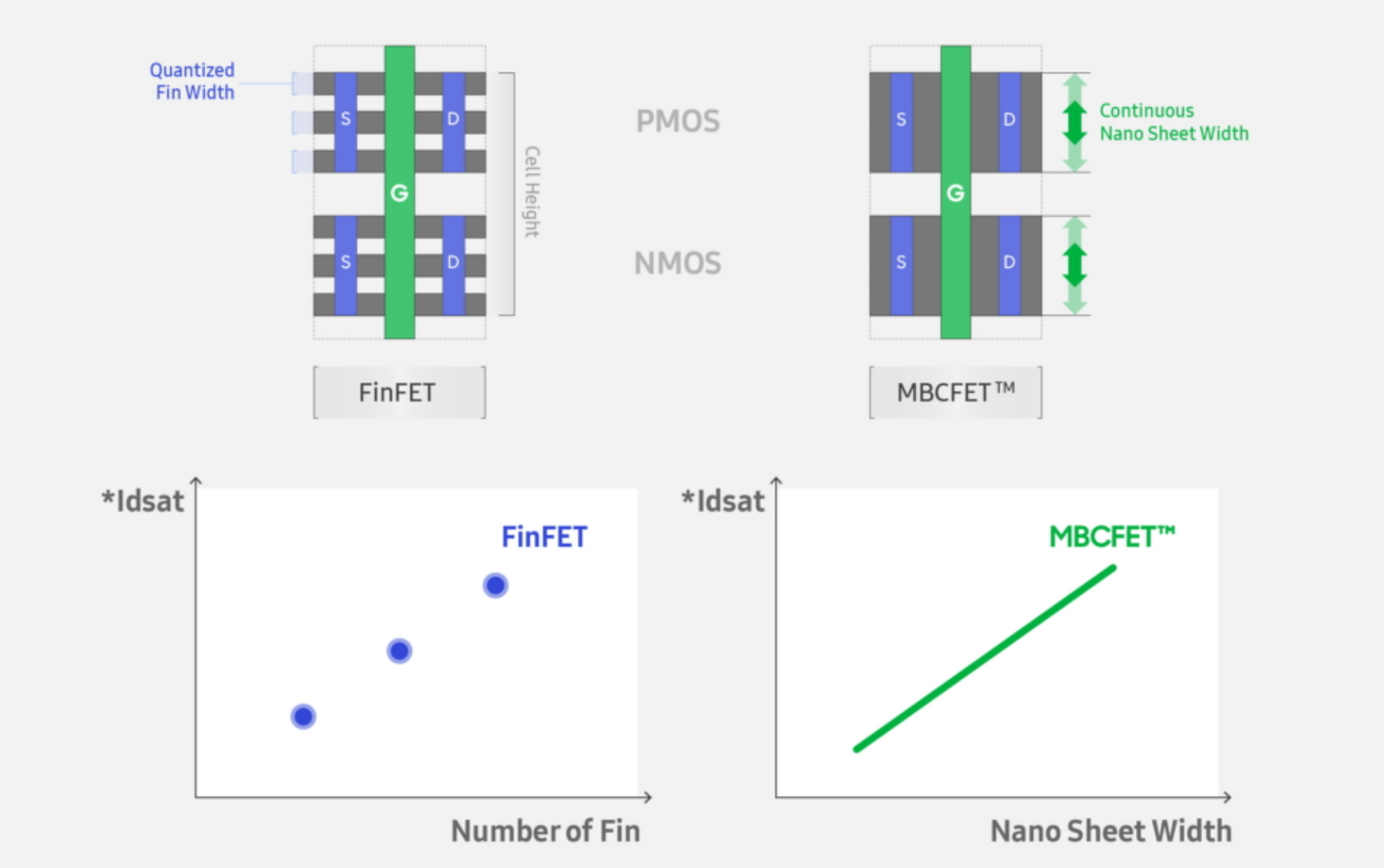
Image from Samsung
Intel has been discussing GAAFETs in technical semiconductor conferences for a number of years, at the International VLSI conference in June 2020, then CTO Dr. Mike Mayberry showcased a diagram with the enhanced electrostatics of moving to a GAA design. At the time we asked about Intel’s timescale for implementing GAA in volume, and were told to expect them ‘within 5 years’. At present Intel’s RibbonFET is due to come with the 20A process, likely to be productized by the end of 2024 based on the roadmaps outlined above.
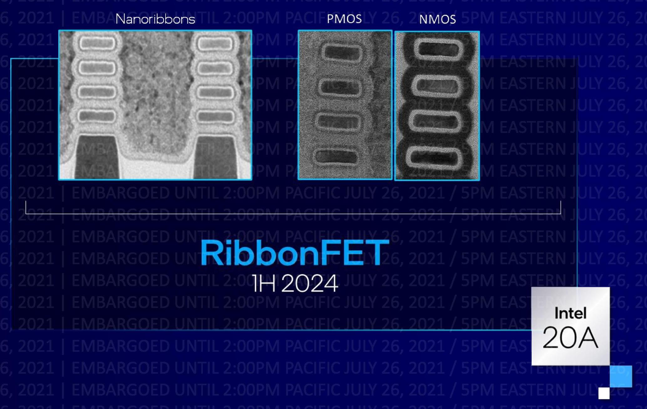
In Intel’s RibbonFET diagrams for this event, they’re showing both PMOS and NMOS devices, as well as what clearly looks like a 4-stack design. Given that I have seen presentations from Intel involving anything from 2-stack to 5-stack at the industry conferences, we confirmed that Intel will indeed be using a 4-stack implementation. The more stacks that are added, the more process node steps are required for manufacturing, and to quote Intel’s Dr. Kelleher, ‘it’s easier to remove a stack than to add one!’. Exactly what is the right number of stacks for any given process or function is still an active area of research, however Intel seems keen on four.
In comparison with Intel’s competitors,
TSMC is expected to transition to GAAFET designs on its 2nm process. At its annual Tech Symposium in August 2020, TSMC confirmed that it would remain on FinFET technology all the way to its 3nm (or N3) process node as it has been able to find significant updates to the technology to allow performance and leakage scaling beyond what was initially expected – N3 is quoted to have up to a 50% performance gain, 30% power reduction, or 1.7x density gain over TSMC N5. Staying on FinFETs, TSMC stated, provides comfort to its customers. Details on TSMC’s N2 have not been disclosed.
Samsung by contrast has stated that it will be introducing its GAA technology with its 3nm process node. Back in Q2 2019, Samsung Foundry announced the first v0.1 development kit of its new 3GAE process node using GAAFETs was being made available to key customers. At the time Samsung predicted volume production by end of 2021, and the latest announcement suggests that while 3GAE will deploy in 2022 internally, main customers may have to wait until 2023 for its more advanced 3GAP process.
To put this into a table:
| Gate-All-Around Transistor Deployment | |||
| AnandTech | Name | Process | Timeframe |
| Intel | RibbonFET | 20A | 2024 |
| 18A | 2025 | ||
| TSMC | GAAFET | N2 / 2nm | EoY 2023? |
| Samsung | MBCFET | 3GAE | 2022 |
| 3GAP | 2023 | ||
By this metric, Samsung might be first to the gate, albeit with an internal node, while TSMC is going to get a lot out of its N5, N4, and N3 nodes first. Around end of year 2023 is when it gets interesting as TSMC may be looking at its N2 designs, while Intel is committed to that 2024 timeframe. The official slide says first half 2024, though as a technology announcement vs product announcement, there is often some lag between the two.
New Technology Features for 2024: PowerVias
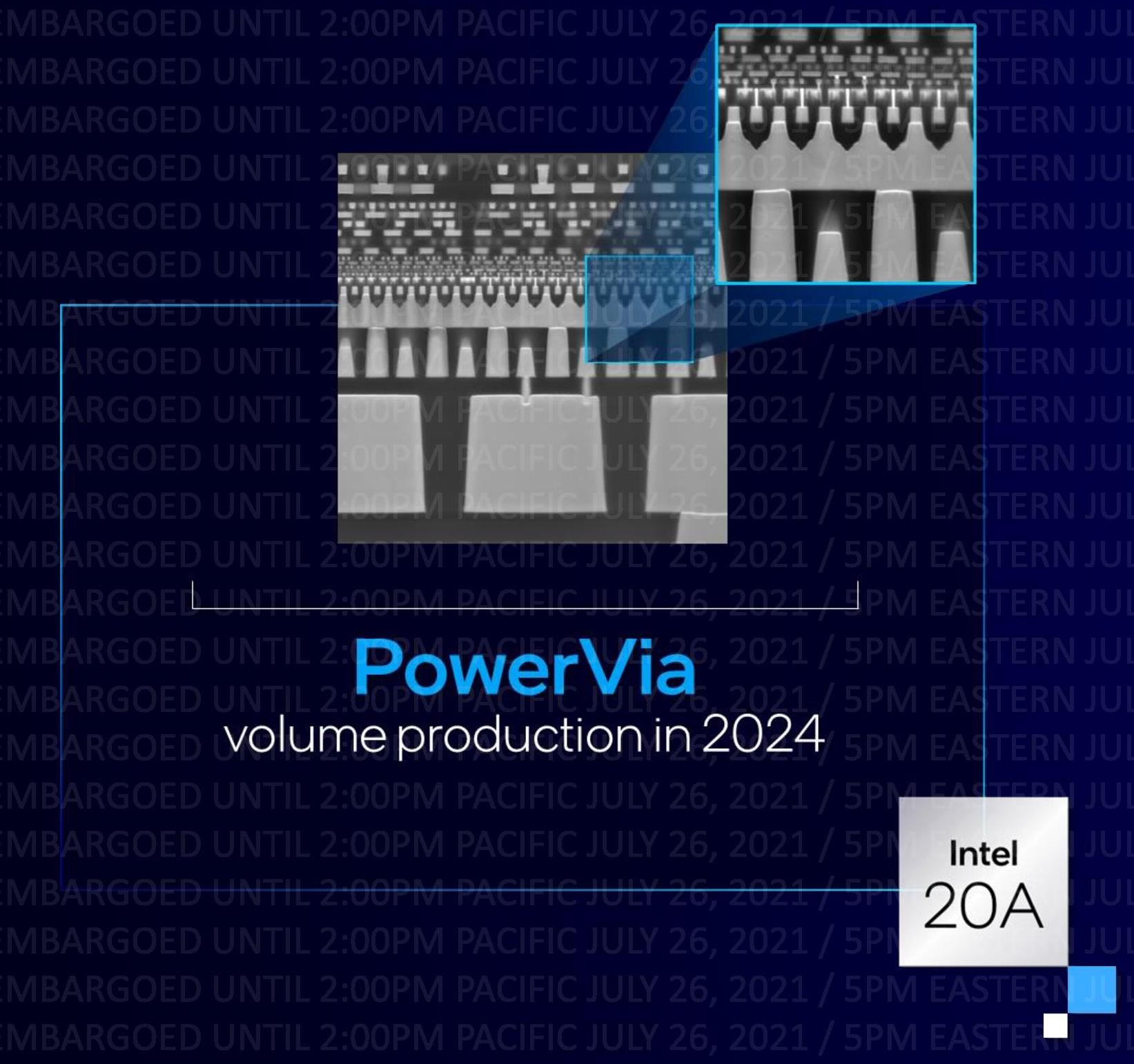
The other arm of Intel’s 20A designs in 2024 is what the company is calling ‘PowerVia’. The concept here pivots the traditional understanding of chip design from a multi-layered cake into a sandwich of sorts.
The manufacturing process of a modern circuit starts the transistor layer, M0, as the smallest layer. Above that, additional metal layers are added at increasing sizes to account for all the wiring needed between the transistors and different parts of the processor (cache, buffers, accelerators). A modern high-performance processor typically has anywhere from 10 to 20 metal layers in its design, with the top layer where the external connections are placed. The chip is then flipped over (known as flip chip) so that the chip can talk to the outside world with those connections on the bottom, and the transistors at the top.
With PowerVias, we now put the transistors in the middle of the design. On one side of the transistors we put the communication wires that allow parts of the chip to talk to each other. On the other side are all the power related connections (along with power gating control). In essence, we moved to a sandwich where the transistors are the filling. This is usually referred to as ‘backside power delivery’ in the industry – PowerVia is Intel’s marketing name.
From a holistic level, we can ascertain that the benefits of this design start with simplifying both the power and the connectivity wires. Typically these have to be designed to ensure there is no signaling interference, and one of the big sources of interference are large power carrying wires, so this takes them out of the equation by putting them on the other side of the chip. It also works the other way – the interference of the interconnected data wires can increase the power delivery resistance, resulting in lost energy and thermals. In this way, PowerVias can help new generations of transistors as drive currents increase by having the power directly there, rather than routed around the connectivity.
There are a couple of hurdles here to mention however. Normally we start manufacturing the transistors first because they are the most difficult and most likely to have defects – if a defect is caught early in the metrology (defect detection in manufacturing), then that can be reported as early in the cycle as possible. By having the transistors in the middle, Intel would now be manufacturing several layers of power first before getting to the tough bit. Now technically these layers of power would be super easy compared to the transistors, and nothing is likely to go wrong, but it is something to consider.
The second hurdle to think about is power management and thermal conductivity. Modern chips are built transistor first into a dozen layers ending with power and connections, and then the chip is flipped, so the power hungry transistors are now at the top of the chip and the thermals can be managed. In a sandwich design, that thermal energy is going to go through whatever ends up on the top of the chip, which is most likely going to be the internal communication wires. Assuming that the thermal increase of these wires doesn’t cause any issues in production or regular use, then perhaps this isn’t so much of an issue, however it is something to consider when heat has to be conducted away from the transistors.
It is worth noting that this ‘backside power delivery’ technology has been in development for a number of years. Across five research papers presented at the VLSI symposium in 2021, imec presented several papers on the technology showing recent advancements when using FinFETs, and in 2019 Arm and imec announced similar technology on an Arm Cortex-A53 built on an equivalent 3nm process in imec’s research facilities. Overall the technology reduces the IR drop on the design, which is becoming increasingly harder to achieve on more advanced process node technologies to drive performance. It will be interesting to see the technology when it is in high volume on high performance processors.


326 Comments
View All Comments
watzupken - Wednesday, July 28, 2021 - link
I think by now we all know that the XXnm naming convention don't mean anything. It does somewhat give you an indication there is some progress in the node, but that's all. In my opinion, I don't really think Intel's current 10nm is in reality, better than TSMC's 7nm. I know the CPU architecture is also a major factor in the efficiency, but just looking at Intel's Tiger Lake H vs AMD's Ryzen 5000H, it is clear that the former consumes a lot more power to reach its performance target. And at the higher power limit, it is not able to decisively pull itself away from the Ryzen processor. Even Alder Lake is rumoured to launch with a PL2 value of 228W, despite using the improved 10nm SuperFin is quite a high number compared to a proper 16 cores Ryzen 5950X.nadim.kahwaji - Wednesday, July 28, 2021 - link
Excellent Article, that's what keep Anandtech so special, i hope the other topis (Especially Graphics ;) ) will Catch soon..SaolDan - Wednesday, July 28, 2021 - link
This move reminds me of Dewalt when they went from torque to UWO. They couldn't compete in torque so they made up their own unit of measurement so they didn't look bad. 20A makes me think of 20Amps.Spunjji - Thursday, July 29, 2021 - link
Dyson with "air watts", too 😅back2future - Wednesday, July 28, 2021 - link
How do consumers follow these advantages on real systems? TDP and energy efficiency, benchmarking tools from chip companies or reviews of integration into different systems or scores/$ and per years of duty?yankeeDDL - Wednesday, July 28, 2021 - link
4 new nodes in 4 years.Very aggressive.
If they can do it, they might actually regain the tech leadership. Wow, 20A tech in 2025 should bring more cores, significant more speed at less power than today's CPU (and GPUs).
Can't complain if that happens.
NickConrad - Wednesday, July 28, 2021 - link
What happened to the December 2019 roadmap that put a 3nm target on 2025? Is this not an admission that they’ll already miss that target by at least a whole generation?Spunjji - Thursday, July 29, 2021 - link
Looks like it!MDD1963 - Sunday, August 1, 2021 - link
Considering the interval between 14 nm and 10nm mainstream desktop CPUs, I'd recommend we look at one step at a time, lest the next shrink step take an additional 7 years...Oxford Guy - Wednesday, August 11, 2021 - link
I’m more concerned with how much power is going to be sacrificed to pursue the AI/spyware route.That’s Apple’s big thing in particular but it’s an industry-wide trend. Individuals are data, products corporations believe are purchased by them when individuals fork over cash.
We have already seen Apple roll out, for instance, a file system that’s abominably inefficient with hard disks and slower than the old one with flash. Then there are all those groovy black box piggybacked chips. I have read that the preposterously-named T2 is now to be embedded in the M2 CPU, like AMD’s PSP and whatever Intel’s spy chip is called.
A new page in CPU reviews will have to be devoted to how much power and die space is going to AI/spyware tech — like making it easier for the government:corporate complex to not only scan your files and take extremely extensive data about them — but move forward with thought crime like ‘preventative indefinite detention’ — a policy then president Obama laid out in a speech.
China is working to force employees to grin correctly in order for office equipment to work. Ugh.