Intel's Process Roadmap to 2025: with 4nm, 3nm, 20A and 18A?!
by Dr. Ian Cutress on July 26, 2021 5:00 PM ESTSidebar on Intel EUV
In all of these announcements, one thing to highlight is Intel mentioning its relationship with ASML, the sole company that manufactures the EUV machines powering production of leading edge semiconductor manufacturing.
ASML Wilton
ASML is a unique company in that it is the only one that can produce these machines, because the technology behind them is often tied up with its partners and research, but also because all the major silicon manufacturers are heavily invested in ASML. For any other company to compete against ASML would require building a separate network of expertise, a decade of innovation and design, and a lot of capital. None of the major silicon vendors want to disturb this balance and go off on their own, lest it shuts them out of the latest manufacturing technology, and no research fund sees competing against the embedded norm as a viable opportunity. This means that anyone wanting EUV specialist technology has to go to ASML.
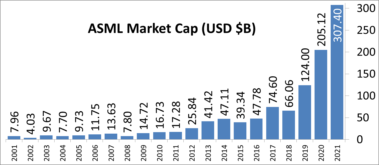
In 2012, it was reported that Intel, Samsung, and TSMC all invested in ASML. This was, at the time, to jumpstart EUV development along with migrating from 300mm wafers to 450mm wafers. While we haven’t moved to 450mm wafers yet (and there are doubts we will any time in the next decade), EUV is now here. Intel’s 2012 investment of $2.1 billion gave them a 10% stake in ASML, with Intel stating that it would continue investing up to a 25% stack. Those stakes are now below the 5% reporting threshold, but all three of the major foundry customers are still big owners, especially as ASML’s market cap has risen from $24 Billion in 2012 to $268 Billion in 2021 (surpassing Intel).
As major investors but also ASML’s customers, the race has been on for these foundries to acquire enough EUV machines to meet demand. TSMC reported in August 2020 that it has 50% of all EUV machines manufactured at ASML for its leading edge processes. Intel is a little behind, especially as none of Intel’s products in the market yet use any EUV. EUV will only intercept Intel’s portfolio with its new Intel 4 process, where it will be used extensively, mostly on the BEOL. But Intel still has to order machines when they need them, especially as there are reports that ASML currently has backorders of 50 EUV machines. In 2021, ASML is expected to manufacture around 45-50 machines, and 50-60 in 2022. The exact number of machines Intel has right now, or has ordered from ASML, is unknown. It is expected that each one has a ~$150m price tag, and can take 4-6 months to install.

With all that being said, Intel’s discussion point today is that it will be the lead customer for ASML’s next generation EUV technology known as High-NA EUV. NA in this context relates to the ‘numerical aperture’ of the EUV machine, or to put simply, how wide you can make the EUV beam inside the machine before it hits the wafer. The wider the beam before you hit the wafer, the more intense it can be when it hits the wafer, which increases how accurately the lines are printed. Normally in lithography to get better printed lines, we move from single patterning to double patterning (or quad patterning) to get that effect, which decreases yield. The move to High-NA would mean that the ecosystem can stay on single patterning for longer, which some have quoted as allowing the industry to ‘stay aligned with Moore’s Law longer’.
| ASML's EUV Shipments | |||||||||||||||||||||
| 2015 | 2016 | 2017 | 2018 | 2019 | 2020 | 2021 | |||||||||||||||
| Actual | 2 | 4 | 10 | 3 | 4 | 5 | 6 | 4 | 7 | 7 | 8 | 4 | 7 | 14 | 8 | 7 | 9 | - | - | ||
| Target (Total) | - | - | - | 20 (18) | 30 (26) | 35 (33) | 45-50 | ||||||||||||||
| 2018 and beyond is split per quarter for actual shipped numbers Data taken from ASML's Financial Reports |
|||||||||||||||||||||
Current EUV systems are NA 0.33, while the new systems are NA 0.55. ASML’s latest update suggests that it expects customers to be using High-NA for production in 2025/2026, which means that Intel is likely going to be getting the first machine (ASML NXE:5000 we think) in mid-2024. Exactly how many High-NA machines ASML intends to produce in that time frame is unknown, as if they flood the market, having the first won’t be a big win. However if there is a slow High-NA ramp, it will be up to Intel to capitalize on its advantage.


326 Comments
View All Comments
watzupken - Wednesday, July 28, 2021 - link
I think by now we all know that the XXnm naming convention don't mean anything. It does somewhat give you an indication there is some progress in the node, but that's all. In my opinion, I don't really think Intel's current 10nm is in reality, better than TSMC's 7nm. I know the CPU architecture is also a major factor in the efficiency, but just looking at Intel's Tiger Lake H vs AMD's Ryzen 5000H, it is clear that the former consumes a lot more power to reach its performance target. And at the higher power limit, it is not able to decisively pull itself away from the Ryzen processor. Even Alder Lake is rumoured to launch with a PL2 value of 228W, despite using the improved 10nm SuperFin is quite a high number compared to a proper 16 cores Ryzen 5950X.nadim.kahwaji - Wednesday, July 28, 2021 - link
Excellent Article, that's what keep Anandtech so special, i hope the other topis (Especially Graphics ;) ) will Catch soon..SaolDan - Wednesday, July 28, 2021 - link
This move reminds me of Dewalt when they went from torque to UWO. They couldn't compete in torque so they made up their own unit of measurement so they didn't look bad. 20A makes me think of 20Amps.Spunjji - Thursday, July 29, 2021 - link
Dyson with "air watts", too 😅back2future - Wednesday, July 28, 2021 - link
How do consumers follow these advantages on real systems? TDP and energy efficiency, benchmarking tools from chip companies or reviews of integration into different systems or scores/$ and per years of duty?yankeeDDL - Wednesday, July 28, 2021 - link
4 new nodes in 4 years.Very aggressive.
If they can do it, they might actually regain the tech leadership. Wow, 20A tech in 2025 should bring more cores, significant more speed at less power than today's CPU (and GPUs).
Can't complain if that happens.
NickConrad - Wednesday, July 28, 2021 - link
What happened to the December 2019 roadmap that put a 3nm target on 2025? Is this not an admission that they’ll already miss that target by at least a whole generation?Spunjji - Thursday, July 29, 2021 - link
Looks like it!MDD1963 - Sunday, August 1, 2021 - link
Considering the interval between 14 nm and 10nm mainstream desktop CPUs, I'd recommend we look at one step at a time, lest the next shrink step take an additional 7 years...Oxford Guy - Wednesday, August 11, 2021 - link
I’m more concerned with how much power is going to be sacrificed to pursue the AI/spyware route.That’s Apple’s big thing in particular but it’s an industry-wide trend. Individuals are data, products corporations believe are purchased by them when individuals fork over cash.
We have already seen Apple roll out, for instance, a file system that’s abominably inefficient with hard disks and slower than the old one with flash. Then there are all those groovy black box piggybacked chips. I have read that the preposterously-named T2 is now to be embedded in the M2 CPU, like AMD’s PSP and whatever Intel’s spy chip is called.
A new page in CPU reviews will have to be devoted to how much power and die space is going to AI/spyware tech — like making it easier for the government:corporate complex to not only scan your files and take extremely extensive data about them — but move forward with thought crime like ‘preventative indefinite detention’ — a policy then president Obama laid out in a speech.
China is working to force employees to grin correctly in order for office equipment to work. Ugh.