Update on Intel Sapphire Rapids in 2022: Q1 for Production, Q2 for Ramp, H1 Launch
by Dr. Ian Cutress on June 29, 2021 9:00 AM EST- Posted in
- CPUs
- Intel
- 10nm
- DDR5
- Xeon Scalable
- PCIe 5.0
- Sapphire Rapids
- 10ESF
- AMX

In the news cycle today, Intel is announcing an update to its planned deployment of its next generation Xeon Scalable platform known as Sapphire Rapids. Sapphire Rapids is the main platform behind the upcoming Aurora supercomputer, and set to feature support for leading edge technologies such as DDR5, PCIe 5.0, CXL, and Advanced Matrix Extensions. The announcement today is Intel reaffirming its commitment to bringing Sapphire Rapids to market for wide availability in the first half of 2022, meanwhile early customers are currently operating with early silicon for testing and optimization.
In a blog post by Lisa Spelman, CVP and GM of Intel’s Xeon and Memory Group, Intel is getting ahead of the news wave by announcing that additional validation time is being incorporated into the product development cycle to assist with top tier partners and customers to streamline optimizations and ultimately deployment. To that end, Intel is working with those top tier partners today with early silicon, typically ES0 or ES1 using Intel’s internal designations, with those partners helping validate the hardware for issues against their wide ranging workloads. As stated by former Intel CTO Mike Mayberry in the 2020 VLSI conference, Intel’s hyperscale partners end up testing 10-100x more use cases and edge cases than Intel can validate, so working with them becomes a critical part of the launch cycle.

As the validation continues, Intel works with its top tier partners for their specific monetizable goals and features that they’ve requested, so that when the time comes for production (Q1 2022) and ramp (Q2 2022), and a full public launch (1H 2022), those key partners are already benefiting from working close with Intel. Intel has stated that as more information about Sapphire Rapids becomes public, such as at upcoming events like Hot Chips in August or Intel’s own event in October, there will be a distinct focus on benchmarks and metrics that customers rely upon for monetizable work flows, which is in part what this cycle of deployment assists with.
Top tier partners getting early silicon 12 months in advance, and then deploying final silicon before launch, is nothing new. It happens for all server processors regardless of source, so when we finally get a proper public launch of a product, those hyperscalers and HPC customers have already had it for six months. In that time, those relationships allow the CPU vendors to optimize the final bits to which the general public/enterprise customers are often more sensitive.
It should be noted that a 2022 H1 launch of Sapphire Rapids hasn’t always been the date in presentations. In 2019, Ice Lake Xeon was a 2020 product and Sapphire Rapids was a 2021 product. Ice Lake slipped to 2021, but Intel was still promoting that it would be delivering Sapphire Rapids to the Aurora supercomputer by the end of 2021. In an Interview with Lisa Spelman in April this year, we asked about the close proximity of the delayed Ice Lake to Sapphire Rapids. Lisa stated that they expected a fast follow on with the two platforms - AnandTech is under the impression that because Aurora has been delayed repeatedly, and that the ‘end of 2021’ was a hard part of Intel’s latest contract with Argonne on the machine for key deliverables. At Computex 2021, Spelman announced in Intel’s keynote that Sapphire Rapids would be launching in 2022, and today’s announcement reiterates that. We expect general availability to be more within the end Q2/Q3 timeframe.
It’s still coming later than expected, however it does space the Ice Lake/Sapphire Rapids transition out a bit more. Whether this constitutes an additional delay depends on your perspective; Intel contends that it is nothing more than a validation extension, whereas we are aware that others may ascribe the commentary to something more fundamental, such as manufacturing. It's no secret that the level of manufacturing capacity Intel has for its 10nm process, or particularly 10nm ESF which is what Sapphire Rapids is built on, is not well known beyond ‘three ramping fabs’ announced earlier this year. Intel appears to be of the opinion that it makes sense for them to work closer with their key hyperscaler and HPC customers, who account for 50-60%+ of all Xeons sold in the previous generation, as a priority before a wider market launch to focus on their monetizable workflows. (Yes, I realize I’ve said monetizable a few times now; ultimately it’s all a function revenue generation.)
As part of today’s announcement, Intel also lifted the lid on two new Sapphire Rapids features.
First is Advanced Matrix Extensions (AMX), which has technically been announced before, and there is plenty of programming documentation about it already, however today Intel is confirming that AMX and Sapphire Rapids are the initial pairing for this technology. The focus of AMX is matrix mutliply, enabling more machine learning compute performance for training and inference in Intel’s key ‘megatrend markets’, such as AI, 5G, cloud, and others. Also part of the AMX disclosures today is some level of performance – Intel is stating that early Sapphire Rapids silicon with AMX, at a pure hardware level, is enabling at least a 2x performance increase over Ice Lake Xeon silicon with AVX512. Intel was keen to point out that this is early silicon without any additional software enhancements on Sapphire Rapids. AMX will form part of Intel’s next-gen DL Boost portfolio at launch.
The second feature is that Intel is integrating a Data Streaming Accelerator (DSA). Intel has also had documentation about DSA on the web since 2019, stating that it is a high-performance data copy and transformation accelerator for streaming data from storage and memory or to other parts of the system through a DMA remapping hardware unit/IOMMU. DSA has been a request from specific hyperscaler customers, who are looking to deploy it within their own internal cloud infrastructure, and Intel is keen to point out that some customers will use DSA, some will use Intel’s new Infrastructure Processing Unit, while some will use both, depending on what level of integration or abstraction they are interested in.
Yesterday we learned that Intel will be offering versions of Sapphire Rapids with HBM integrated for every customer, with the first deployment of those going to Aurora. As mentioned, Intel is confirming that they will be disclosing more details at Hot Chips in August, and at Intel’s own Innovation event in October. There may also apparently be some details about the architecture before that date as well, according to today’s press release.
Realted Reading
- Hot Chips 33 (2021) Schedule Announced: Alder Lake, IBM Z, Sapphire Rapids, Ponte Vecchio
- Intel to Launch Next-Gen Sapphire Rapids Xeon with High Bandwidth Memory
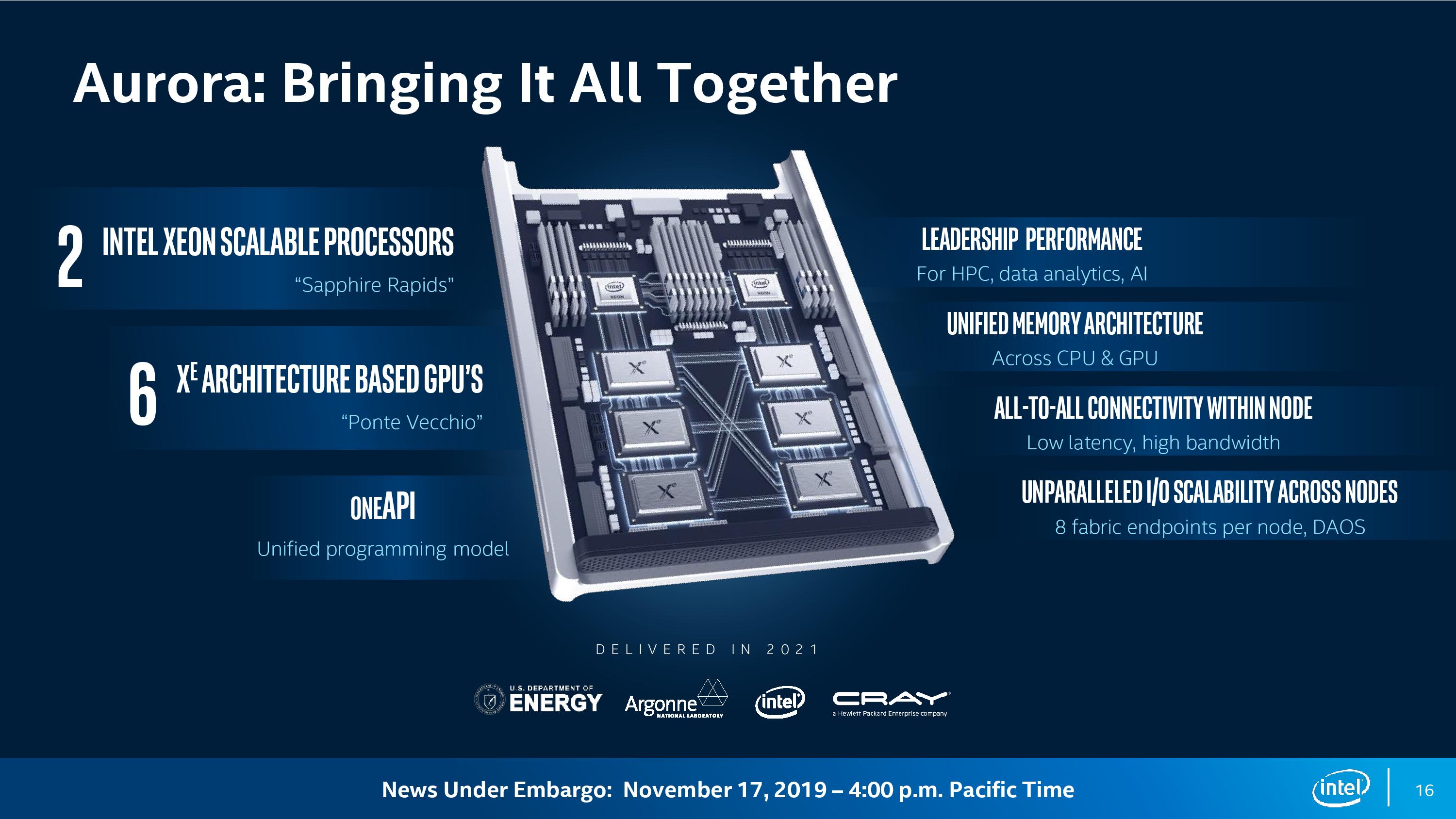
- Intel’s 2021 Exascale Vision in Aurora: Two Sapphire Rapids CPUs with Six Ponte Vecchio GPUs
- Intel Updates ISA Manual: New Instructions for Alder Lake, also BF16 for Sapphire Rapids
- Intel’s Full Enterprise Portfolio: An Interview with VP of Xeon, Lisa Spelman
- Intel 3rd Gen Xeon Scalable (Ice Lake SP) Review: Generationally Big, Competitively Small


34 Comments
View All Comments
mode_13h - Sunday, July 4, 2021 - link
> in my experience FP16 just isn't good enough in training scenarios.People say BF16 converges faster, but Nvidia did pretty well with FP16 for both the P100, V100, and Turing. They didn't get around to adding BF16 until Ampere.
> 2. AMX will make BF16 matrix multiplications on Sapphirelake much easier compared
> to Cooperlake since we would only need one instruction to multiply 2 matrix tiles
From what I've seen, it supports only dot-product, not proper matrix-multiply. They also haven't specified the throughput or latency. Don't assume you can issue one of those every cycle.
> Mathematically, you still need to read every single matrix element from RAM at least once
But you can hold one of the matrices on-chip (i.e. the model, which doesn't change) and just read the data that's being forward propagated. Because models are too big to fit entirely on-chip, you break them into pieces and run a batch of data through, before loading and applying the next piece.
The reason this helps is that models are typically much bigger that the data being propagated through them.
And as for AMX and convolutions, it can just load the new elements for each window position. Therefore, it potentially has a much lighter impact on the cache hierarchy.
> Therefore it is fundamentally a data flow and bandwidth constrained problem not a
> FPU constrained problem
Nvidia's P100 had 720 GB/s of memory bandwidth to support 21.2 fp16 TFLOPS. The V100 increased memory bandwidth to 900 GB/s to support 125 tensor fp16 TFLOPS, and you claim that was a waste???
Given these numbers, an Intel Xeon should be nowhere close to bandwidth-constrained if you're smart about your data movement.
As I said, a lot of AI chips have just DDR4 memory, because they're smarter about using their on-die SRAM to avoid excessive data movement.
SystemsBuilder - Tuesday, July 6, 2021 - link
I’m probably not very clear so I’ll try again, being even more technical and hopefully more precise this time – sorry for the long post.1. Intel manual (https://software.intel.com/content/www/us/en/devel... page 3-17. TMUL multiplication instruction TDPBF16PS is named dot product BUT in the context of matrix tiles that means tile x tile matrix multiplication, tile being a sub matrix. In other words TDPBF16PS multiplies 2 tile matrices of BF16 floats together and accumulate the result to a third tile – see detailed pseudo code on page 3-18, note in particular the 3 level nested for loop. Like the standard dgemm mm algorithm for multiplying 2 matrices, the full matrix multiplication is a series of tile * tile (in the literature sometimes called block matrices) multiplications going over rows and columns of tiles in the standard way until all tiles are multiplied the right way. Difference between AVX-512 FP32 (besides format) is that TDPBF16PS does a full tile x tile multiplication in 1 instruction while we need about 16 * 16 = 256 vfmadd231ps to achieve a tile x tile multiplication, producing a 16x16 FP32 float tile (ignoring the obvious size advantage BF16 have over/FP32). As both you and I pointed out what remains to be seen is the TDPBF16PS clock cycle Throughput and Latency. vfmadd231ps is a about 4-7 cycles (depending on port 0 or 5 etc.) and you can cut that in half one a CPU with 2 FMAs (high end Xeons have 2 AVX-512 FMAs). We’ll just have to wait for the TDPBF16PS Throughput and Latency numbers to do a final comparison.
But this is just 1 matrix multiplication in isolation… Neural net quires a tons of serially dependent once and that is the crux.
2. The mathematical nature of neural net training (not just inference that is much simpler) – example: basic 3 layer neural net, applying standard forward and backwards propagation. Restraining myself abit here (removing activation function, activation function derivatives, Grad, matrix hadamults, add, subs, scalar mults and other stuff, focusing on the core of the compute complexity: the matrix multiplications themselves).
a) A forward pass of one sample batch matrix X0, requires W1*X0 -> W2*X1 -> W3*X2 -> X3 sequential and completely serially dependent matrix multiplication (X are the signal matrices, W are the weight matrices, number = layer matrix belong to, -> is the mathematical dependency between two ops). In addition to this you need to calculate and store activation function, activation function derivatives matrices at each layer. This means you need to stream X0 (mini batch) through the compute engine and calculate and store approximately 11-13 matrices each forward propagation pass iteration and, as mentions before, the L1$/L2$ cache is not big enough to keep all of them in cache permanently.
b) Further when you are finally done with forward propagation you need to take the final layer output (ignoring Grad etc calc stuff again for simplicity) and run the matrix result backwards to calculate error (D): D3W3^T -> D2 -> D2W2^T -> D1 and lastly update the weights(W): D3X3^T -> W3, D2X2^T -> W2, D1X1^T -> W1. Also serially dependent and updated every backwards propagation iteration (one layer compute result is mathematically depended on the previous layer result), in total about another 10-12 matrices are computed and stored.
c) Lastly you now have to repeat this for the next X0 mini batch until exhausted all samples in the training data set AND then you have to do this last for loop step again hundreds of times (i.e. all EPOCs).
So the so called “training model” (activation + it’s derivative, W, error, and their deltas), is about 20-24+ matrices for a 3 layer network (depending on the exact flavor of algorithm and optimization used) freshly calculated and updated every iteration based on the next mini batch X0 and can in total take up 10s of MB up to GBs+ – just for the model. And you need them all in each iteration and no one is less important than another, because they are serially dependent of each other.
My point with this is that math is math. Doesn’t matter how smart you do things unless you change the forward backwards propagation and stochastic gradient decent (or some variation thereof - there are many…) algorithm to something fundamentally different, you are stuck with these matrix calc serial dependencies AND the memory bandwidth bottle neck that comes with it.
At the macro level the best you can hope for is to keep all activation X, W, Error etc matrices (plus potentially/ideally? “helper” matrices, e.g. delta W/error) in cache since they are updated and read so frequently, but X0 changes with every min batch in the inner loop so… Also W and Delta W matrices tend to be the largest in the entire net of matrices so there is that going on too…
3. we stared this as comparison between intel generations Icelake/Cooperlake and Sapphire Rapids. Comparing with Nvidia's highly parallel and specialized SMID architecture (and different caching all together) with intel's general purpose CPU is is a very different discussion - and a very long one - so I'll stick to the original scope.
4. there is some new news though about Sapphire Rapids that may help to explain how intel have addressed the memory bandwidth challenge to try to keep up with the TMUL. https://videocardz.com/newz/intel-sapphire-rapids-... Sapphire Rapids L1$: 48KB/core, L2$: 2MB/core, L3 cache is 3.75MB/core (75 Mbyte for 20 cores - this is a big upgrade) shared + the HBMe upgrade will help, but what is the latency and B/W going to be?
mode_13h - Wednesday, July 7, 2021 - link
Thanks for the link to the Intel docs, but it doesn't work for me. I hope you're right that it can do more than just dot-product.As for your example, you focused only on training and skipped convolution. When inferencing with convolution layers, the output is much smaller than the weights. So, it's possible to apply a chunk of the weights to a portion of a batch of input data, save the intermediates, and repeat. This saves you from having to reload all the weights for every inference sample. GPUs continue to gain benefits from extremely large batch sizes, up to 512 images, in some cases.
SystemsBuilder - Wednesday, July 7, 2021 - link
Here is the link to "Intel Architecture Instruction Set Extensions Programming Reference" talking about the Tiles and Tile Multiplications in chapter 3 with my references about TDPBF16PS above page 3-17, 3-18: https://software.intel.com/content/www/us/en/devel... if it does not work just search for Intel Architecture Instruction Set Extensions Programming Reference or use the link posted in the main article above.Yes, as I wrote earlier inference is much easier since you only need fully trained W matrices that should be stable and should be possible to keep in cache BUT that is just inference after training is done. Mathematically, inference is basically a subset of training with just one single forward propagation pass a(W1*X0) -> a(W2*X1) -> a(W3*X2) -> X3 per mini batch (if you infer in mini batch format) just calculating activation functions at each layer (a) without calculating activation derivates, Grads, etc and without the entire backwards pass and no iterations. The hard time consuming work is training! Magnitudes more complex than inference.
In inference you can even go down in resolution from BF16 to Byte and change activation functions to something like much simpler, almost binary 1/0 across the board. And AMX has a byte Tile multiplication: TDPBUUD as well for that! You can define tiles as a signed/unsigned byte data type so now each signal is just a byte long, compressing the format even further from 16 bits to 8 bits. Inference with byte data type should get a 2x speed up from just data format compression.
Convolutional neural network (CNN) is a sub class of general deep neural nets that I talked about in my 3 layer example so what I wrote above in general about training deep neural net applies to them too (broadly speaking) - CNN have very interesting properties that make them very attractive in many specific AI applications - images recognition etc.
mode_13h - Thursday, July 8, 2021 - link
Thanks for the updated link. That works. I'll take a little time to update my knowledge of AMX, before posting more about it.> The hard time consuming work is training!
Yeah, but once you've trained a model, you can inference with it billions of times. Many accelerators specialize on either training or inference. A device needn't be equally competent at both, and inference is the bigger market (also the easier problem).
JayNor - Tuesday, June 29, 2021 - link
"Intel is keen to point out that some customers will use DSA, some will use Intel’s new Infrastructure Processing Unit, while some will use both"The IPU might contain its own DSA, right? My understanding is current generation of IPUs would be expected to have ethernet IO and PCIE IO, plus some ASIC or FPGA to accelerate encode, decode, encryption ...
Will DSA on SPR be doing the CXL coherency DMA transfers?
Will DSA DMA be used for all the GPU to GPU transfers on the Aurora nodes?
mode_13h - Friday, July 2, 2021 - link
> Will DSA DMA be used for all the GPU to GPU transfers on the Aurora nodes?It seems that all of the GPUs are directly connected. So, probably not, unless the GPUs have their own built-in DSAs.
JayNor - Friday, July 2, 2021 - link
The GPU coherency is maintained by the host processor home agent, so I suspect all the gpu to gpu data movements on a single node will need to go through the host.zamroni - Wednesday, June 30, 2021 - link
Will it be epycly thread ripped again by ryzen amd?Just like avx 512, that dl boost is effectively useless for servers because the corporate customers will use gpu or tpu, which is many times more powerful, if they are seriously use ai.
Intel should simply uses the transistor budget for caches
EthiaW - Wednesday, June 30, 2021 - link
Will Intel launch an independent DPU as Nvidia did? They already have the DSA.