Arm Announces Mobile Armv9 CPU Microarchitectures: Cortex-X2, Cortex-A710 & Cortex-A510
by Andrei Frumusanu on May 25, 2021 9:00 AM EST- Posted in
- SoCs
- CPUs
- Arm
- Smartphones
- Mobile
- Cortex
- ARMv9
- Cortex-X2
- Cortex-A710
- Cortex-A510
A new CI-700 Coherent Interconnect & NI-700 NoC For SoCs
Finally, the last new announcement of the day is a new interconnect and network-on-chip generation. The last time Arm had announced a mobile/client interconnect was back in in 2015 with the CCI-550. The reason for the large gap between IPs, in Arm’s own words, is that ever since Arm’s introduction of the DSU in its CPU complexes, there really hasn’t been any need for a cache coherent interconnect in the market. While that’s eyebrow-raising from a GPU perspective, it makes perfect sense from a CPU perspective, as coherency between CPU cores was the primary driver for such interconnects until then.
With the advent of new more complex computing platforms, such as NPUs, accelerators, and hopeful more use of GPUs in cache-coherent fashions, Arm saw a need gap in its portfolio and decided to update its client-side interconnect IP.
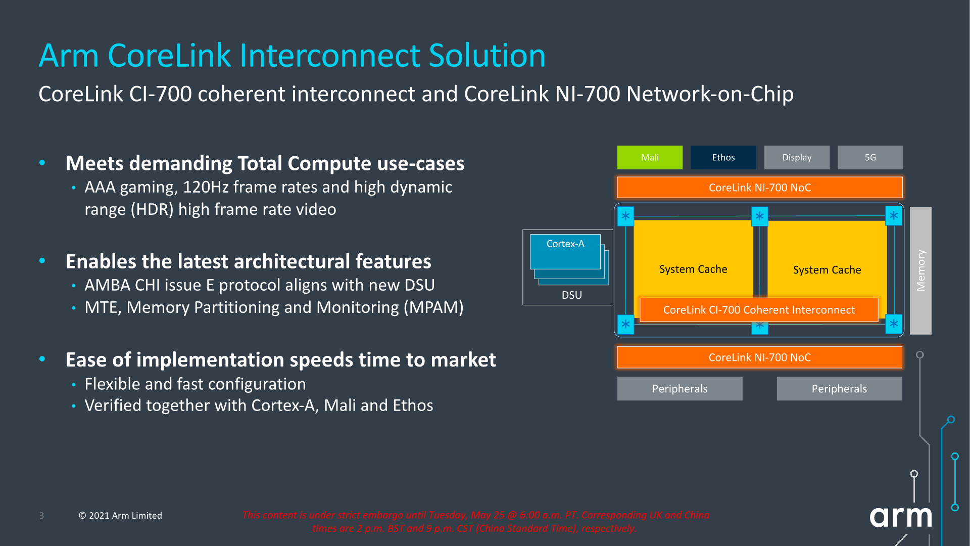
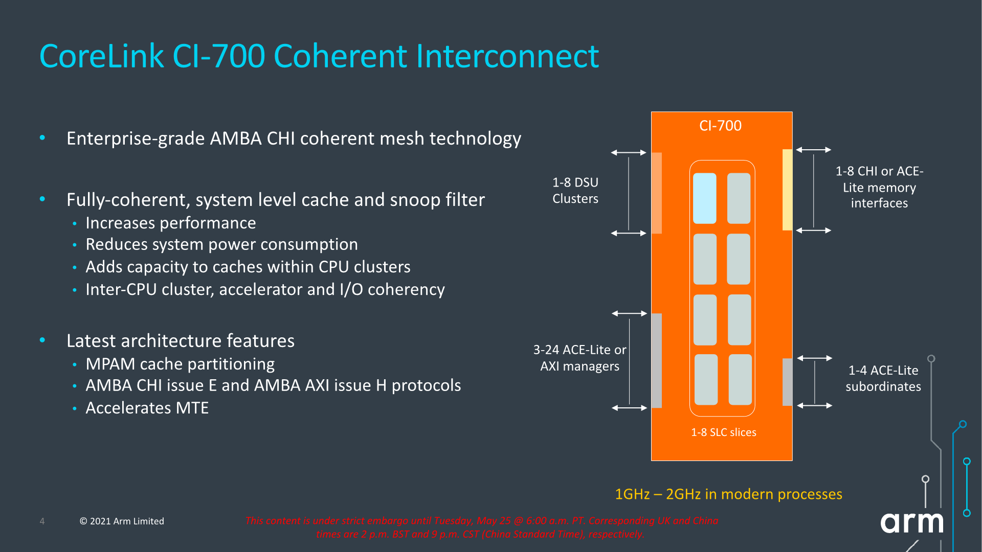
The new CI-700 is a mobile and client optimised variant of Arm’s infrastructure CMN mesh network, implementing important new interoperability with the new IP announced today, such as the new DSU or CPU cores.
The new mesh interconnect scales up from 1 to 8 DSU clusters, and supports up to 8 memory controllers, and also introduces innovations such as a system level cache.
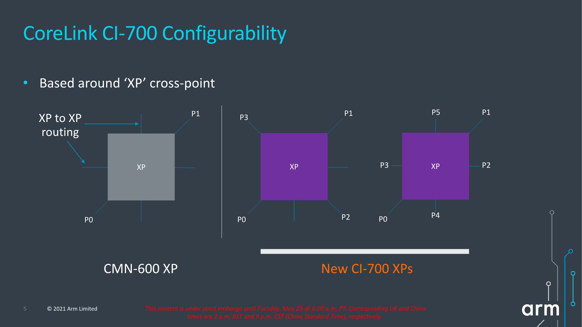
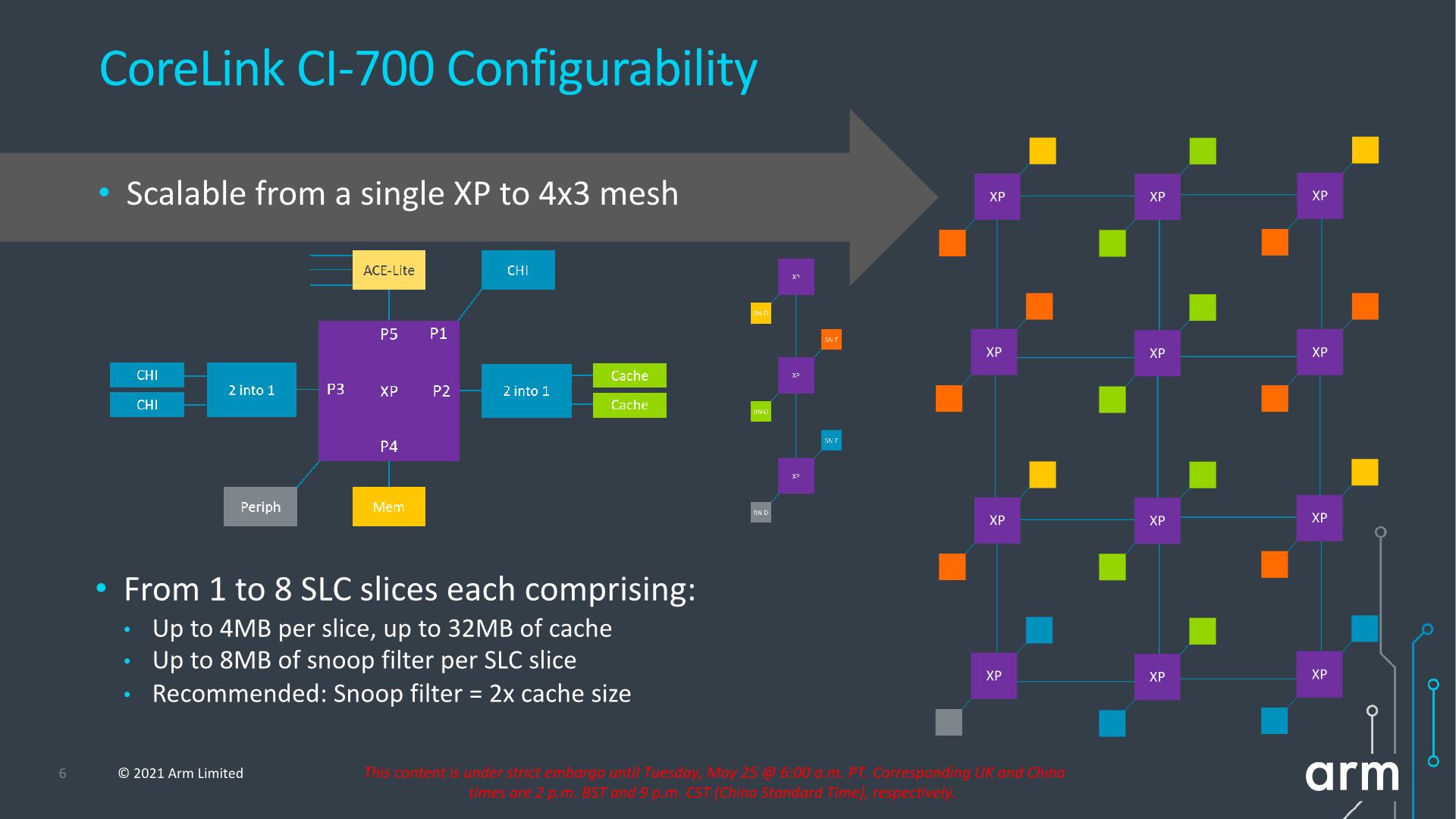
The mesh network topology and building blocks is very similar to what we’ve seen in the CMN infrastructure IP, in that “points” in the mesh are comprised of “cross-points” or “XP”. One differentiation that’s unique to the client mesh implementation is that XPs can have more attached connectivity ports, trading in routing connection paths. The new IP can also be configured as just a sole XP with no real mesh so to speak of, or essentially a 1x1 mesh configuration. This can grow up to a 4x3 mesh in the largest possible configuration.
The mesh supports from 1 to 8 SLC slices, with up to 4MB per slice for a total of 32MB, and snoop filter SRAM with coverage of up to 8MB address space per slice. It’s noted that generally Arm recommends 1.5-2x of coverage of the underlying private cache hierarchies of the mesh clients.
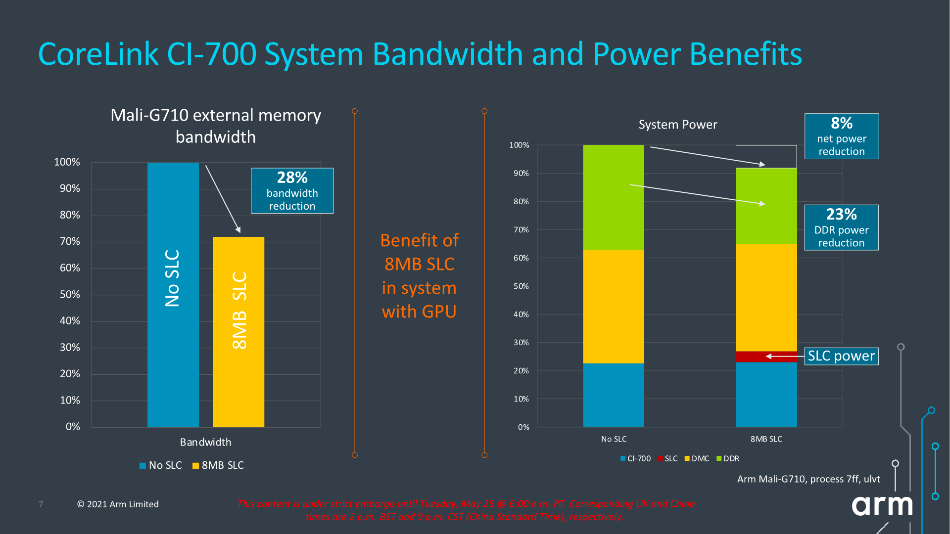
The SLC can server as both a bandwidth amplifier as well as reducing external memory/DRAM transactions, reducing system power reduction.
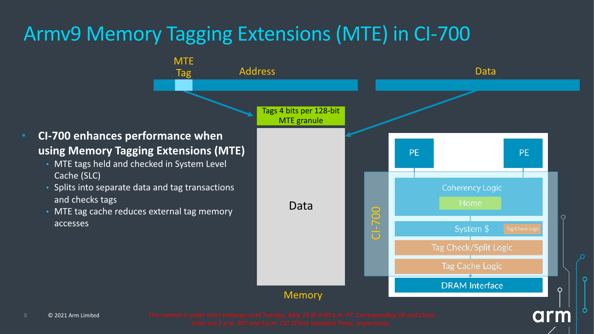
We see a reiteration of the support for MTE, allowing for this generation of IPs to support the feature across the new CPU IP, the DSU, and the new cache coherent interconnect.
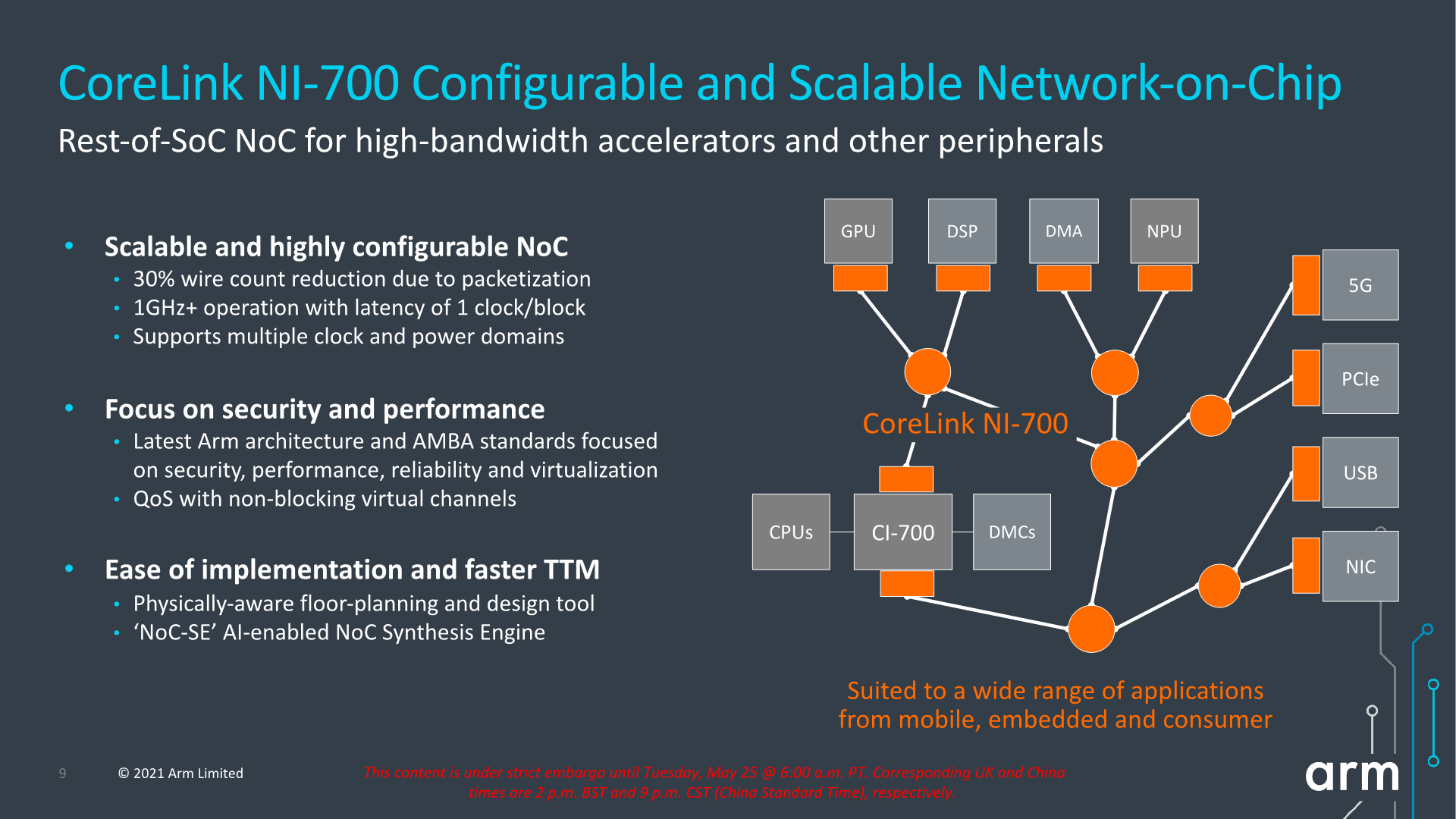
Alongside the new CI-700 coherent interconnect, we’re also seeing a new NI-700 network-on-chip for non-coherent data transfers between a SoC’s various IP blocks. The big new improvements here is the introduction of packetization for data transfers, which leads to a reduction of wires and thus improves area efficiency of the NoC on the SoC.
Overall, the new system IP announced today is very interesting, but the one question that’s one has to ask oneself is exactly who these net interconnects are meant for. Over the last few years, we’ve seen essentially every major mobile vendor roll out their own in-house cache-coherent interconnect IP, such as Samsung’s SCI or MediaTek’s MCSI, and other times we don’t see vendors talk about their in-house interconnects at all (Qualcomm). Due to almost everybody having their own IP, I’m not sure what the likelihood would be that any of the big players would jump back to Arm’s own solutions – if somebody were to adopt it, it would rather be amongst the smaller name vendors and newcomers to the market. From a business and IP portfolio perspective, the new designs make a lot of sense and allows to have the building blocks to create a mostly Arm-only SoC, which is an important item to have on the menu for Arm’s more diverse customer base.


181 Comments
View All Comments
Ppietra - Tuesday, May 25, 2021 - link
I believe that he was talking about the overall SPEC2006 score and not just SPECint. Still he would be wrong about the X1 score, which would be 50 and not 40 (probably a typo).Anyway a 16% improvement for X2 over X1 would mean a score of 58 which, like he said, would still be behind the A13 performance core and well behind the 72 score for the A14.
X1 is already being manufactured at 5nm, so it makes no sense to factor in a transition from 7nm.
Wilco1 - Tuesday, May 25, 2021 - link
Cortex-X1 can reach 3.2GHz in Samsung's 5nm process but the power is too high: https://images.anandtech.com/doci/16463/2100-volta...TSMC 5nm is faster and lower power, which allows for higher frequencies. At a conservative 3.3GHz X2 would have a combined score of ~66.7 (only 7% slower than A14).
Ppietra - Tuesday, May 25, 2021 - link
That is not how it works!First of all you have no idea what would be the advantage from using TSMC instead of Samsung, so you are just throwing numbers with no substance. Secondly, X1 energy consumption is already very high (it is less efficient than the A14 Firestorm core), so no, there doesn’t seem to be a lot of room to improve X2 clock speed to 3.3GHz. Thirdly even with your assumption you would still have X2 performing worse than a 1 year old core
Wilco1 - Tuesday, May 25, 2021 - link
We absolutely do know. TSMC 5nm is ~15% faster than 7nm at the same power (or 30% lower power at the same frequency). We know that SD865+ achieves 3.1GHz on 7nm and that the frequency gain from A13 on 7nm to A14 on 5nm was around 13%. So 3.3GHz should be feasible on 5nm without increasing power.The point is that TSMC 5nm will give a significant perf/power boost (that A14 already benefits from). And that means the gap has narrowed to only one generation rather than 2.
melgross - Tuesday, May 25, 2021 - link
It’s not that simple. The cores would require a bit of a redesign for the different process, and each design would fare differently. Some might get a good boost, and others may not.michael2k - Tuesday, May 25, 2021 - link
You're comparing the X2 to the A14? I mean, if we're lucky we will see the X2 in 2022 alongside the A16. The A15 will be released this year, in 2021. We already have some X1 baselines:https://www.anandtech.com/show/16463/snapdragon-88...
So in terms of generation:
2021 X1 not competitive with the 2019 A13 now
2021 X1 competitive with the 2019 A13 on TSMC 5nm
2021 X1 not competitive with the 2021 A15 (est 10% boost to hit 70 SPECint)
2022 X2 competitive with the 2020 A14 on TSMC 5nm
2022 X2 not competitive with the 2021 A15
That still sounds like a 2 generation gap to me. The real problem isn't fundamentally the core, but the OEM choosing not to use a 2x2 design (2 X1 and 2 A77) or (2 X2 and 2 A710), so even if the cores get faster each generation, overall performance is hobbled by using 3 medium cores instead of a pair of higher performance X1 or X2 cores.
Fulljack - Wednesday, May 26, 2021 - link
it's cat and mouse, really. Apple release their phones in late Q3, while Samsung S-series are released in late Q1. there's 5 to 6 month difference.Ppietra - Wednesday, May 26, 2021 - link
Nothing of what you said gives you any data to infer about a transition from Samsung to TSMC.SD865+ does not use a X1 core, as such you have no commonality to make that kind jump in analysis, secondly the X1 core already consumes significantly more than the SD865+ core, so clearly there is no much room to increase clock speed from that perspective. If you want to increase clock speed you need to keep power consumption under control.
Wilco1 - Wednesday, May 26, 2021 - link
These are different generations of the same microarchitecture from the same design team with the same frequency capability (as reported by AnandTech). So yes there is obvious commonality.We also know this microarchitecture is capable of higher frequencies, for example AnandTech reports Cortex-X1 can reach 3.2GHz. The main problem is power however, which is what limited Cortex-X1 on Samsung's process. TSMC 5nm reduces power by 30% which enables higher clock speeds.
Ppietra - Wednesday, May 26, 2021 - link
actually they aren’t different generations from the same microarchitecture. The next generation for the A77 is the A78. The X1 goes for a bigger core design, and as such consumes more.Being capable of higher frequencies doesn't mean that Qualcomm (, etc) finds it viable to use those higher frequencies in a smartphone SoC...
NODE power reduction is stated for same performance and microarchitecture (which X1 is not) and only as an internal TSMC comparison... The data you give tells you nothing about X1 (already at 5nm) transitioning to TSMC. You are making an analysis based on wrong assumptions.