Arm Announces Mobile Armv9 CPU Microarchitectures: Cortex-X2, Cortex-A710 & Cortex-A510
by Andrei Frumusanu on May 25, 2021 9:00 AM EST- Posted in
- SoCs
- CPUs
- Arm
- Smartphones
- Mobile
- Cortex
- ARMv9
- Cortex-X2
- Cortex-A710
- Cortex-A510
New DSU-110 L3 & Cluster: Massively More Bandwidth
Alongside the new CPU microarchitectures, Arm today is also announcing a new L3 design in the form of the new DSU-110. The “DynamIQ Shared Unit” had been the company’s go-to cluster and “core complex” block ever since it was introduced in 2017 with the Cortex-A75 and Cortex-A55. While we’ve seen small iterative improvements, today’s DSU-110 marks a major change in how the DSU operates and how it promises to scale up in cache size and bandwidth.
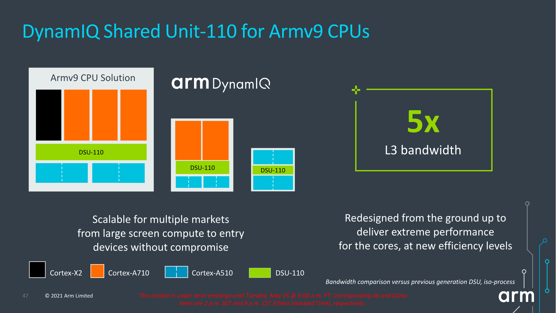
The new DSU-110 is a ground-up redesign with an emphasis on more bandwidth and more power efficiency. It continues to be the core building block for all of Arm’s mobile and lower tier market segments.
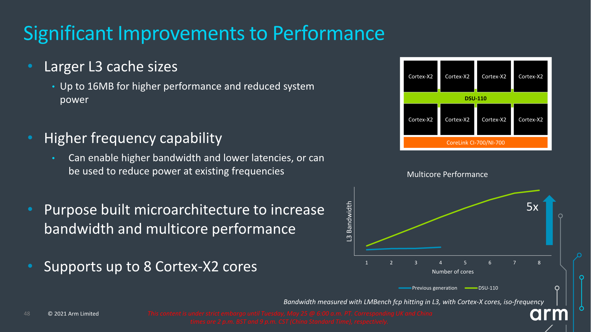
A key metric is of course the increase of L3 cache configuration which will now go up to 16MB this generation. This is of course the high-end of the spectrum and generally we shouldn’t expect such a configuration in a mobile SoC soon, but Arm has had several slides depicting larger form-factor implementations using such a larger design housing up to 8 Cortex-X2 cores. This is undoubtedly extremely interesting for a higher-performance laptop use-case.
The bandwidth increase of the new design is also significant, and applies from single-thread to multi-threaded scenarios. The new DSU-110 promises aggregate bandwidth increases of up to 5x compared to the contemporary design. More interesting is the fact that it also significantly boosts single-core bandwidth, and Arm here actually notes that the new DSU can actually support more bandwidth than what’s actually capable of the new core microarchitectures for the time being.
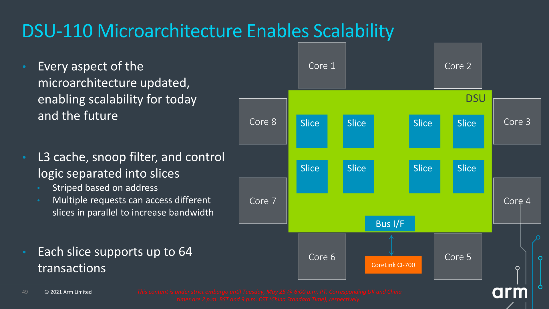
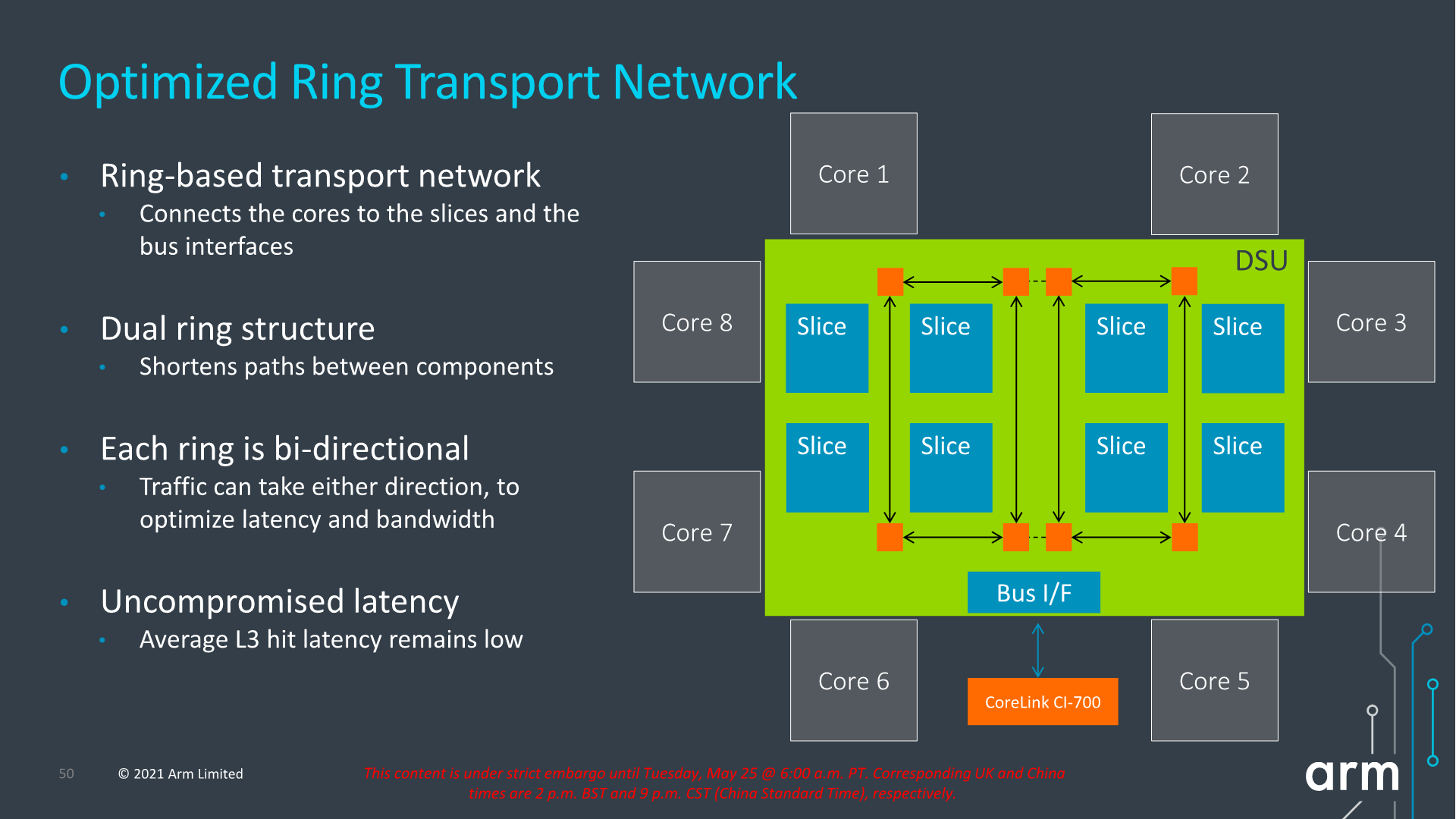
Arm never really disclosed the internal topology of the previous generation DSU, but remarks that with the DSU-110 the company has shifted over to a bi-directional dual-ring transport topology, each with four ring-stops, and now supporting up to 8 cache slices. The dual-ring structure is used to reduce the latencies and hops between ring-stops and in shorten the paths between the cache slices and cores. Arm notes that they’ve tried to retain the same lower access latencies as on the current generation DSU (cache size increases aside), so we should be seeing very similar average latencies between the two generations.
Parallel access increases for bandwidth as well as more outstanding transactions seem to have been also very important in order to improve performance, which seems very exciting for upcoming SoC designs, but also puts into more question the previously presented CPU IPC improvements and exactly how much the new DSU-110 contributes to those numbers.
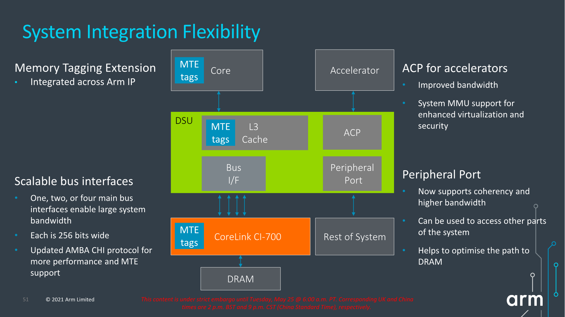
Architecturally, one important change to the capabilities of the DSU-110 is support for MTE tags, a upcoming security and debugging feature promising to greatly help with memory safety issues.
The new DSU can scale up to 4x AMBA CHI ports, meaning we’ll have up to 1024-bit total bi-directional bandwidth to the system memory. With a theoretical DSU clock of around 2GHz this would enable bandwidth of up to 256GB/s reads or writes, or double that when combined, plenty enough to be able to saturate also eventual high-end laptop configurations.

In terms of power efficiency, the new DSU offers more options for low-power operation when in idle situations, implementing partial L3 power-down, able to reduce leakage power of up to 75% compared to the current DSU.
In general idle situations but still having the full L3 powered on, the new design promises up to 25% reduction in leakage power all whilst offering 2x the bandwidth capabilities.
It’s important to note that we’re talking about leakage power here- active dynamic power is expected to generally scale linearly with the bandwidth increase of the new design, meaning 5x the bandwidth would also cost 5x the power. This would be an important factor to note into system power and in general the expected power behaviour of the next-gen SoCs when they’re put under heavy memory workloads.
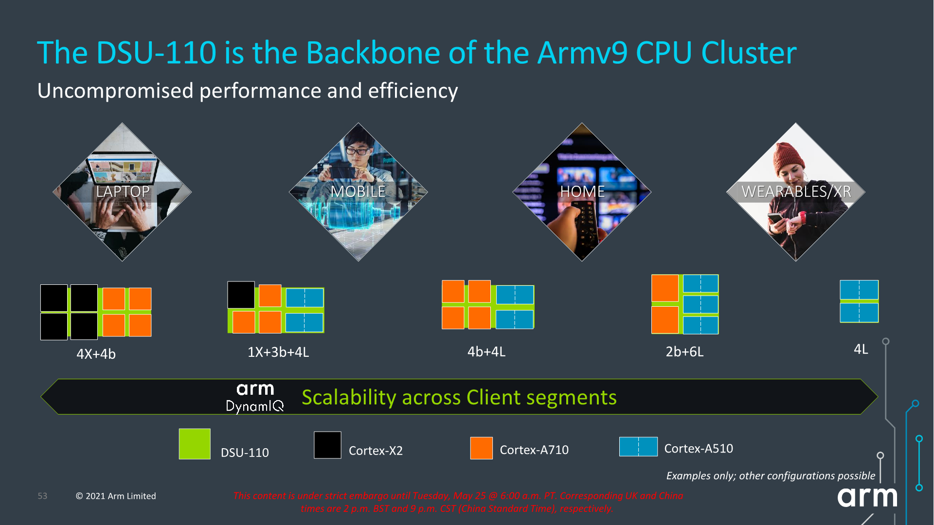
Arm describes the DSU-110 as the backbone of the Armv9 cluster and that seemingly seems to be an apt description. The new bandwidth capabilities are sure to help out both with single-threaded, but also with multi-threaded performance of upcoming SoCs. Generally, the new 16MB L3 capability, while it’s possible somebody might do a high-end laptop SoC configuration, isn’t as exciting as the now finally expected move to a new 8MB L3 on mobile SoCs, hopefully also enabling higher power efficiency and more battery life for devices.


181 Comments
View All Comments
ChrisGX - Monday, May 31, 2021 - link
There is one part of Andrei's analysis of the X2 core that I don't get. I do get the scepticism about ARM's optimistic estimate of a 30% lift in peak performance being on offer given the dismal underperformance of Samsung's 5nm silicon but my reading of what ARM has said is that the 16% performance gain for the X2 is ISO process, i.e. on the same silicon process at the same power and frequency. Am I wrong to read this as (effectively) an IPC gain without an energy cost associated with it? (Let us ignore for the moment such good news will likely be dashed due of Samsung's iffy silicon.) I know that sounds like a very rosy picture but isn't that the picture that ARM painted? In this context I don't get Andrei's suggestion of a lineal increase in power for that peak performance gain.Personally, I find the claim of a 16% performance gain hard to believe (and the 30% number after unspecified silicon process improvements and processor clock boost, presumably, even harder to believe). Still, I want to be clear on what ARM is claiming and what I have missed (if anything). Any comments would be welcome.
ChrisGX - Monday, May 31, 2021 - link
I have just reviewed Andrei's analysis again and I note he referred to a power increase (not a lineal power increase in proportion to the 16% performance increase) drawing particularly attention to the increased cache size.ChrisGX - Wednesday, June 2, 2021 - link
Regarding the projections of a 30% peak performance increase for a premium mobile SoC in 2022 I can't see how to get to that performance number (after a 16% IPC increase) without a) the prime X2 core being clocked at around 3.3GHz - 3.35GHz and b) corresponding silicon process improvements that permit lower voltages (at the increased core frequency). That implies a process that is better than TSMC's N5.For an 8 core X2 based SoC for consumer computers that performs at a peak rate of 1.4x the performance of a Core i5-1135G7 (which would represent a truly stunning level of performance) I think the SoC would have to be clocked at around 3.7GHz - 3.8GHz (again on a process that is markedly better than TSMC's N5). Performance like that, of course, won't come without elevating core and SoC power consumption to a significant degree.
Getting performance outcomes as good as that doesn't seem especially likely to me.
mode_13h - Wednesday, June 2, 2021 - link
Thanks for the analysis. If correct, this could mark the opening of a significant credibility gap, in ARM's projections.ChrisGX - Sunday, June 6, 2021 - link
I just had a look at the PPA Improvements that TSMC has advertised for its N4 process (there are unconfirmed claims that Qualcomm will be using N4 for the next premium SoC for flagship Android mobile phones) and I don't see ARM's projected performance numbers being reached on that process. N3 would do it but we won't see that before 2H2022. Without inviting thermal problems a performance improvement of 24% at 3.2GHz might fall within the bounds of possibility. (Note: Information on the N4 process is thin but I have assumed 7% more performance will be available at the same power compared to N5. With additional performance improvements of 16% from IPC gains - without pushing the power budget - a performance lift of 24% seems feasible.)https://www.anandtech.com/show/16639/tsmc-update-2...
rohn287 - Thursday, December 2, 2021 - link
Just asking, why not use 2-X2 cores with 2 higher clocked A710 and 2 normal A710. This will help reduce heat and increase performance in Android phones. Similar to Apples approach.The Futuristic - Saturday, April 2, 2022 - link
I know it's too late for comment, but the processors with this core have just entered the market. Depending on them and comparing them with Apple A15 E cores especially, I think they should start using cortex A710 as E cores instead of cortex A55. Apple E cores consumes around 0.44watt, cortex A78 in dimensity 1200 at 6nm uses 1.16W for same performance. So A710 is 30% efficient for same and taking it even further on 5nm. It will close the gap between Apple E cores and cortex cores. So 2x cortex X2 + 4x cortex A710 configured CPU, will catch Apple A15 in multi-core atleast.yeeeeman - Wednesday, May 11, 2022 - link
we're getting very close to the cortex x3 announcement.yeeeeman - Saturday, June 4, 2022 - link
seems like arm is missing the end of may announcements this year. anyone knows why?