Intel 11th Generation Core Tiger Lake-H Performance Review: Fast and Power Hungry
by Brett Howse & Andrei Frumusanu on May 17, 2021 9:00 AM EST- Posted in
- CPUs
- Intel
- 10nm
- Willow Cove
- SuperFin
- 11th Gen
- Tiger Lake-H
CPU Tests: Microbenchmarks
Core-to-Core Latency
As the core count of modern CPUs is growing, we are reaching a time when the time to access each core from a different core is no longer a constant. Even before the advent of heterogeneous SoC designs, processors built on large rings or meshes can have different latencies to access the nearest core compared to the furthest core. This rings true especially in multi-socket server environments.
But modern CPUs, even desktop and consumer CPUs, can have variable access latency to get to another core. For example, in the first generation Threadripper CPUs, we had four chips on the package, each with 8 threads, and each with a different core-to-core latency depending on if it was on-die or off-die. This gets more complex with products like Lakefield, which has two different communication buses depending on which core is talking to which.
If you are a regular reader of AnandTech’s CPU reviews, you will recognize our Core-to-Core latency test. It’s a great way to show exactly how groups of cores are laid out on the silicon. This is a custom in-house test built by Andrei, and we know there are competing tests out there, but we feel ours is the most accurate to how quick an access between two cores can happen.
In terms of the core-to-core tests on the Tiger Lake-H 11980HK, it’s best to actually compare results 1:1 alongside the 4-core Tiger Lake design such as the i7-1185G7:
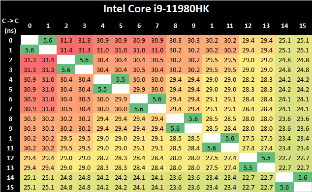

What’s very interesting in these results is that although the new 8-core design features double the cores, representing a larger ring-bus with more ring stops and cache slices, is that the core-to-core latencies are actually lower both in terms of best-case and worst-case results compared to the 4-core Tiger Lake chip.
This is generally a bit perplexing and confusing, generally the one thing to account for such a difference would be either faster CPU frequencies, or a faster clock of lower cycle latency of the L3 and the ring bus. Given that TGL-H comes 8 months after TGL-U, it is plausible that the newer chip has a more matured implementation and Intel would have been able to optimise access latencies.
Due to AMD’s recent shift to a 8-core core complex, Intel no longer has an advantage in core-to-core latencies this generation, and AMD’s more hierarchical cache structure and interconnect fabric is able to showcase better performance.
Cache & DRAM Latency
This is another in-house test built by Andrei, which showcases the access latency at all the points in the cache hierarchy for a single core. We start at 2 KiB, and probe the latency all the way through to 256 MB, which for most CPUs sits inside the DRAM (before you start saying 64-core TR has 256 MB of L3, it’s only 16 MB per core, so at 20 MB you are in DRAM).
Part of this test helps us understand the range of latencies for accessing a given level of cache, but also the transition between the cache levels gives insight into how different parts of the cache microarchitecture work, such as TLBs. As CPU microarchitects look at interesting and novel ways to design caches upon caches inside caches, this basic test proves to be very valuable.
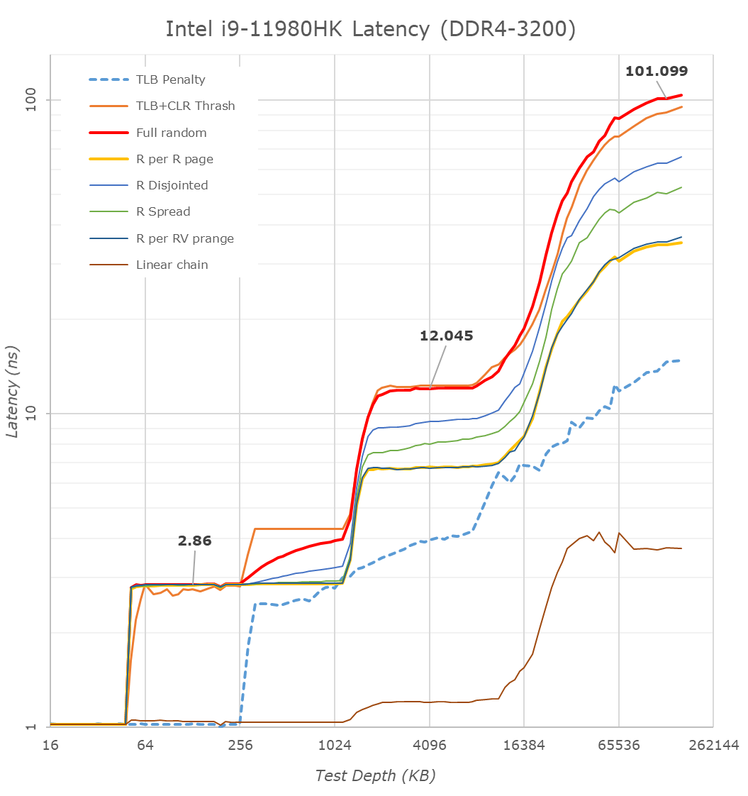
What’s of particular note for TGL-H is the fact that the new higher-end chip does not have support for LPDDR4, instead exclusively relying on DDR4-3200 as on this reference laptop configuration. This does favour the chip in terms of memory latency, which now falls in at a measured 101ns versus 108ns on the reference TGL-U platform we tested last year, but does come at a cost of memory bandwidth, which is now only reaching a theoretical peak of 51.2GB/s instead of 68.2GB/s – even with double the core count.
What’s in favour of the TGL-H system is the increased L3 cache from 12MB to 24MB – this is still 3MB per core slice as on TGL-U, so it does come with the newer L3 design which was introduced in TGL-U. Nevertheless, this fact, we do see some differences in the L3 behaviour; the TGL-H system has slightly higher access latencies at the same test depth than the TGL-U system, even accounting for the fact that the TGL-H CPUs are clocked slightly higher and have better L1 and L2 latencies. This is an interesting contradiction in context of the improved core-to-core latency results we just saw before, which means that for the latter Intel did make some changes to the fabric. Furthermore, we see flatter access latencies across the L3 depth, which isn’t quite how the TGL-U system behaved, meaning Intel definitely has made some changes as to how the L3 is accessed.


229 Comments
View All Comments
Spunjji - Thursday, May 20, 2021 - link
He measured the power consumption, you pillock. It's right there in the review. Nice work getting your FUD on the front page though, round of applause for gondaft.If Tiger Lake H will be better in "the right chassis", Intel really should have thought of that when they supplied this one. As things stand, it's clear that this chassis wasn't causing the CPU to throttle at 45W, so the only way it would perform better is in a chassis that allows for 65W - at which point you'd find AMD's CPUs performing better, too...
5j3rul3 - Monday, May 17, 2021 - link
It's a big step to intelM1 and Ryzen 5000 are powerful, Intel need more pros to getting the leading performance
mode_13h - Monday, May 17, 2021 - link
This is definitely what Rocket Lake should've been. If they just put this chip in a desktop package, so it could be run with a desktop power budget and cooling, it'd sure be a lot more interesting than it is inside a laptop.Exotica - Monday, May 17, 2021 - link
Yields may have been the primary concern.mode_13h - Monday, May 17, 2021 - link
I get why they didn't do it, but it's clear to me this chip really wants to be a desktop CPU.whatthe123 - Monday, May 17, 2021 - link
it's probably more that they've tweaked their 10nm to hit high boost at the cost of efficiency. I think they increased their gate pitch with "superfin" so you end up with more performance scaling but also more power use. considering how far behind their desktop chips are compared to 7nm chips from AMD they may just be crippling efficiency across the board to get performance parity while their fabs lag behind. they don't seem to have high hopes for 10nm considering their target for market leadership is 2024 with 7nm.laptop users generally stick with bursty operations or video games and in both cases raw throughput isn't as much of a concern. average user would probably not notice or even benefit from the high ST burst performance, but anyone planning on using it professionally would probably be better off with cezanne.
Spunjji - Tuesday, May 18, 2021 - link
It would certainly be able to stretch its legs better there. It would be interesting to see whether it could handle running those higher boost clocks across more cores with a higher TDP. Guess we'll find out with Alder Lake.Lucky Stripes 99 - Monday, May 17, 2021 - link
I thought the same. This chip in a mini-STX case with a desktop cooler would make a great portable system. However, if it is having thermal issues with a full-size workstation laptop, it'll likely struggle in the smallest of SFF cases like the NUC.Azix - Monday, May 17, 2021 - link
the laptop doesn't look that that big. A nuc would have more vertical space for the cooling for example. It would also be easier to throw that heat out.mode_13h - Monday, May 17, 2021 - link
Uh, the mini-STX NUCs don't really have much space. Everything is packed in pretty tightly. Furthermore, they usually top out at 28 W.For Coffee Lake, Intel made a larger system they called a "NUC", but I think they had actual Nvidia graphics cards in them and were bigger than a lot of mini-PCs.