Intel to Invest $3.5 Billion USD into Foveros and EMIB Production in Rio Rancho
by Dr. Ian Cutress on May 3, 2021 12:00 PM EST
At a news conference today, Intel has announced that its Rio Rancho campus in New Mexico will be getting an investment of $3.5 billion USD for an expansion of its current state-of-the-art facilities for the company to roll out its new Foveros packaging technology in volume for its own products as well as its customers. This comes on top of the $20 billion USD that Intel has committed to two new fabrication plants in its Ocotillo campus in Arizona for wafer production. In partnership with New Mexico state and local government, the new investment is expected to provide 1000 construction jobs over three years, 700 permanent technical positions at the company, and 3500 ancillary positions in the area when the facility is fully functional.
Modern Processor Manufacturing
During a time when the semi-conductor market is experiencing overwhelming demand for its products, there are a lot of cogs in the supply chain to ensure that everything is moving in the right direction as well as a growth in capacity across the board. Typically when the industry talks about supply constraints, it most often directed towards the ability to produce the silicon wafers and chips, however the post-production element of that is also important: being able to build this silicon into useable product for each market also needs to be scaled to meet demand, and this is also a point where we are seeing a squeeze in the industry.

Intel's current Rio Rancho campus
Today’s announcement of $3.5 billion USD for an expanded Intel facility in Rio Rancho is along those lines. This expanded facility won’t be building silicon wafers or silicon chips, but instead will be taking chips that are already made (made either at Intel or other foundries like TSMC) and constructing them into a package which is then sold onto partners. This facility will be specializing in construction using Intel’s new 3D packaging technology, also known as Foveros, as well as continuing investments in Intel’s Embedded Multi-Die Interconnect Bridge (EMIB) technology.
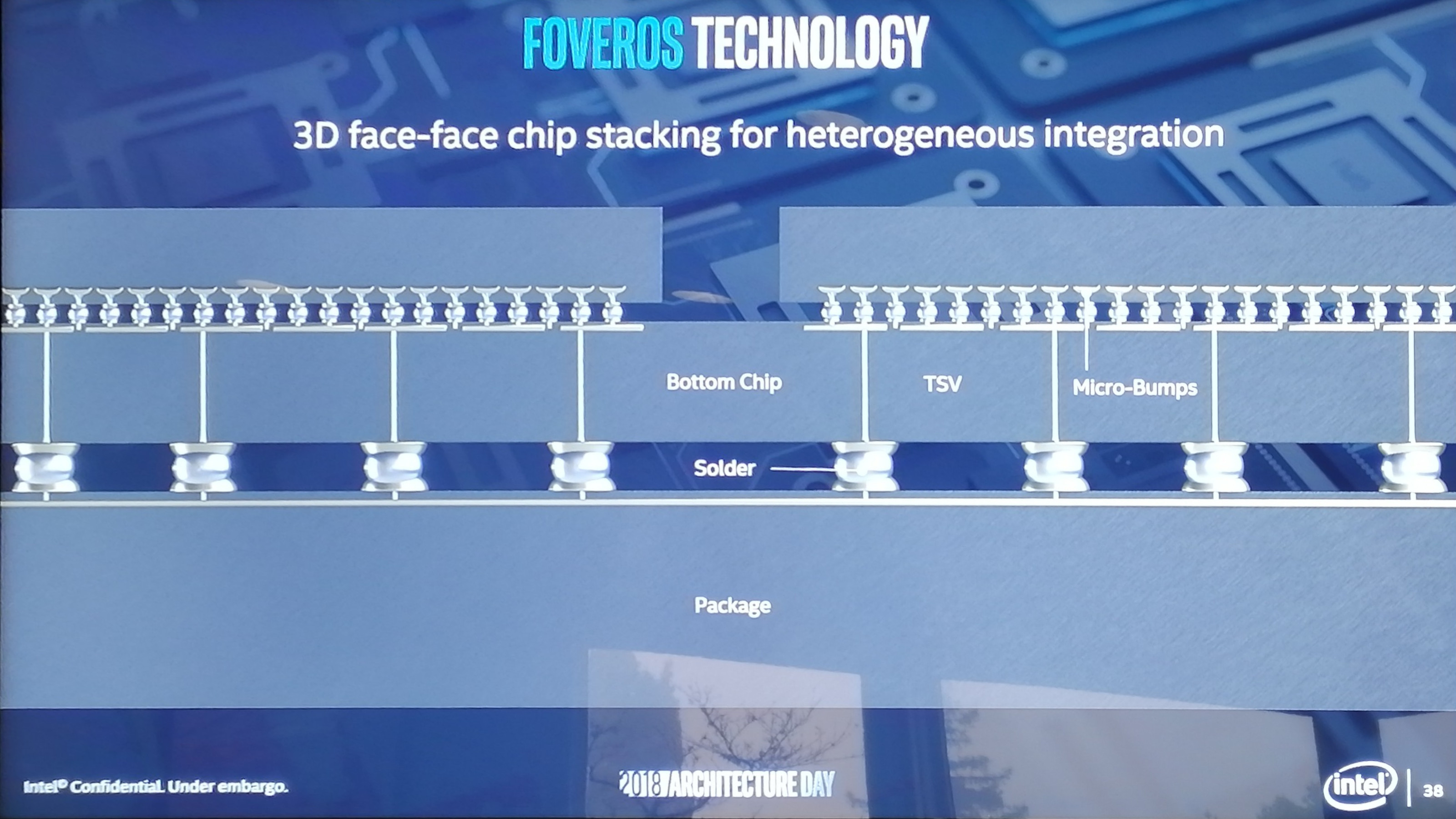
Foveros is a die-to-die packaging technology that connects two chips together. Intel has already enabled Foveros on one technology in the market, a laptop processor called Lakefield, as well as a product currently in production, the high-performance compute processors called Ponte Vecchio, set to be used in the Aurora supercomputer as one of America’s largest computing projects to date. So far these two projects are specialized, with comparatively few units compared to Intel’s major product lines. With the expanded facility at Rio Rancho, Intel intends to invest in its capability to roll out products co-designed with its advanced packaging technologies like Foveros on a wider scale.

CEO Pat Gelsinger with a Ponte Vecchio XPU using EMIB+Foveros
Construction for the new expansion is set to start in late 2021, and be production-ready by late 2022. Intel has confirmed to AnandTech that the facility is aimed purely at building its advanced 3D packaging and testing facilities for end products, rather than R&D into some of Intel’s other on-site activities, such as 3D XPoint, which had been postulated in the media.
We did ask Intel whether the new facility would be focused on 3D packaging solely for Intel’s own product lines, or whether it would be made available to Intel’s future Foundry customers as part of its Intel Foundry Services (IFS) program – Intel declined to comment, but stated that the facility will be managed by Keyvan Esfarjani, SVP and GM of Intel’s Manufacturing and Operations. Intel has also stated that it will purchase renewable energy to meet 100% of the electricity use at the expanded facility.
Intel’s press release on the news focuses specifically on Foveros deployment, however we are led to believe that EMIB production is also going to be bolstered by the expansion, given both fall under Intel’s advanced 3D packaging capabilities. Intel told us to consider this purely as a packaging and testing facility expansion, something that Intel already does a lot of, akin to what other companies might call an OSAT under their fabless models.
Related Reading
- Intel’s Future 7nm FPGAs To Use Foveros 3D Stacking
- Intel Next-Gen 10-micron Stacking: Going 3D Beyond Foveros
- An Interconnected Interview with Intel’s Ramune Nagisetty: A Future with Foveros
- Intel's Interconnected Future: Combining Chiplets, EMIB, and Foveros
- Intel’s New IDM 2.0 Strategy: $20b for Two Fabs
- What Products Use Intel 10nm? SuperFin and 10++ Demystified


20 Comments
View All Comments
Unashamed_unoriginal_username_x86 - Monday, May 3, 2021 - link
Real men get US government subsidiesYojimbo - Monday, May 3, 2021 - link
Lots of things get US government subsidies.. Tesla, for example. And TSMC gets Taiwanese government subsidies. Especially when TSMC and UMC were being set up, the industrial campuses were set up by the government, the research was funded by the government, and the government made billions of investment in the 90s.Having semiconductor manufacturing in the US is a national security issue. It deserves US government subsidy if the situation is that there is not enough US manufacturing with out. The situation will only get worse if China, with massive government subsidy, gets its manufacturing off the ground. And if we wait too long then we won't have the manufacturing or engineering knowhow for to scale up our semiconductor manufacturing quickly, leaving us completely vulnerable if China invades Taiwan.
Otritus - Tuesday, May 4, 2021 - link
I'm fairly certain Unashamed_unoiriginal_username_x86's comment was a play on Jerry Sanders' (cofounder of AMD) "real men have fabs"Santoval - Tuesday, May 4, 2021 - link
"..leaving us completely vulnerable if China invades Taiwan.They will. It's not a question of "if" but "when".
Roland00Address - Monday, May 3, 2021 - link
Why would AMD be getting subsidies? All fabs companies are arguing for subsidies because the current market is messed up with under-demand in the 2000s creating under-supply for the bean counters did not want to overbuild and thus a virtuous / viceful cycle was created and we now in 2021 understand this was not efficent.If AMD wanted back into the fab business they would be arguing for subsidies. But right now it is Intel, TSMC, Samsung, and perhaps Global Foundries arguing for subsidies of the leading fabs as are a dozen plus older fabs where many companies have moved to newer processes but companies that currently have older designs want those fabs to stay open and not update for they do not want to respin that chip someplace else for it would include a re-design.
JayNor - Monday, May 3, 2021 - link
Yeah, part of their IFS plan includes offering their advanced packaging. That may be the main draw until they get geared up to do co-packaged optics. They've done more emib at this point.EthiaW - Monday, May 3, 2021 - link
So in which site is the Lakefeild gotten Feveros now?Smell This - Tuesday, May 4, 2021 - link
So this is the 'active interposer' with chiplets that are stacked along side the CPU die?
Samus - Wednesday, May 5, 2021 - link
It's too bad Wisconsin tossed the coin and lost with Foxconn when Intel et al would have probably taken those tax credits for a legitimate site.cucotvapk - Monday, May 24, 2021 - link
The most stunning part of this application is, it can prepared to isolate HQ joins for chronicles on both normal customers and Real-debrid accounts. It offers an immense variety of stuff that customers can peruse. https://cucotv.com/download/ It isn't hard to download CucoTV on Android-based devices anyway needs a functioning helper for other stage contraptions.