AI Meets Chipmaking: Applied Materials Incorporates AI In Wafer Inspection Process
by Anton Shilov on March 19, 2021 1:00 PM EST- Posted in
- Semiconductors
- Applied Materials
- ExtractAI
- Enlight
- SEMVision
Advanced system-on-chip designs are extremely complex in terms of transistor count and are hard to build using the latest fabrication processes. In a bid to make production of next-generation chips economically feasible, chip fabs need to ensure high yields early in their lifecycle by quickly finding and correcting defects.
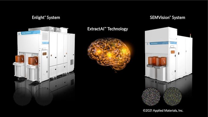
But finding and fixing defects is not easy today, as traditional optical inspection tools don't offer sufficiently detailed image resolution, while high-resolution e-beam and multibeam inspection tools are relatively slow. Looking to bridge the gap on inspection costs and time, Applied Materials has been developing a technology called ExtractAI technology, which uses a combination of the company's latest Enlight optical inspection tool, SEMVision G6/G7 e-beam review system, and deep learning (AI) to quickly find flaws. And surprisingly, this solution has been in use for about a year now.
UPDATE 3/21: Applied Materials sent in an email to clarify that Extract AI can work not only with the SEMVision G7, but also with the SEMVision G6.
"Applied’s new playbook for process control combines Big Data and AI to deliver an intelligent and adaptive solution that accelerates our customers’ time to maximum yield," said Keith Wells, group vice president and general manager, Imaging and Process Control at Applied Materials. "By combining our best-in-class optical inspection and eBeam review technologies, we have created the industry’s only solution with the intelligence to not only detect and classify yield-critical defects but also learn and adapt to process changes in real-time. This unique capability enables chipmakers to ramp new process nodes faster and maintain high capture rates of yield-critical defects over the lifetime of the process."
Defect Detection: A Crucial Step in Chip Manufacturing
As a highly competitive industry, the semiconductor industry is also extremely time sensitive. Modern companies have to develop new chips, bug fix them, and then launch them all on fairly tight schedules. Nowadays it takes years to develop an advanced chip and several months to actually fabricate a batch. One of the most crucial time parameters is time to yield, which is to say being able to provide a large number of chips with high enough yields. A chip designer may have the most efficient architecture around, but if they cannot get it made in high volumes, they'll still lose out on money and market share. Even foundries feel this pinch, as the time needed to fix defects and bring lines up to snuff represents millions of dollars in equipment depreciation alone – one week of a 3nm fab downtime is expected to cost $25 million in unamortized depreciation costs. So achieving acceptable time to yield metrics heavily depends on a fab's ability to detect and fix yield-killing defects.

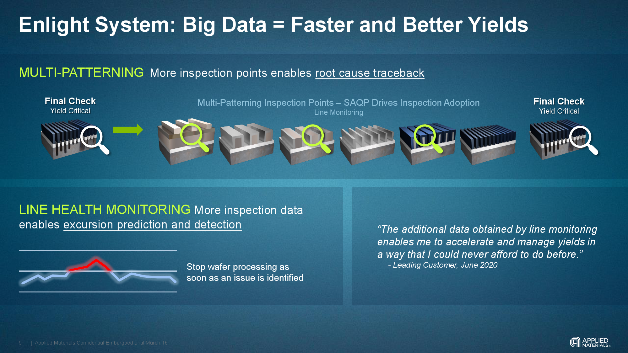
Since the majority of advanced SoCs are made using extremely small fabrication processes – many of which rely on multi patterning and/or extreme ultraviolet (EUV) lithography – it is getting very tough to detect defects. Applied Materials says that the number of process steps increased by 48% from 2015 to 2021.
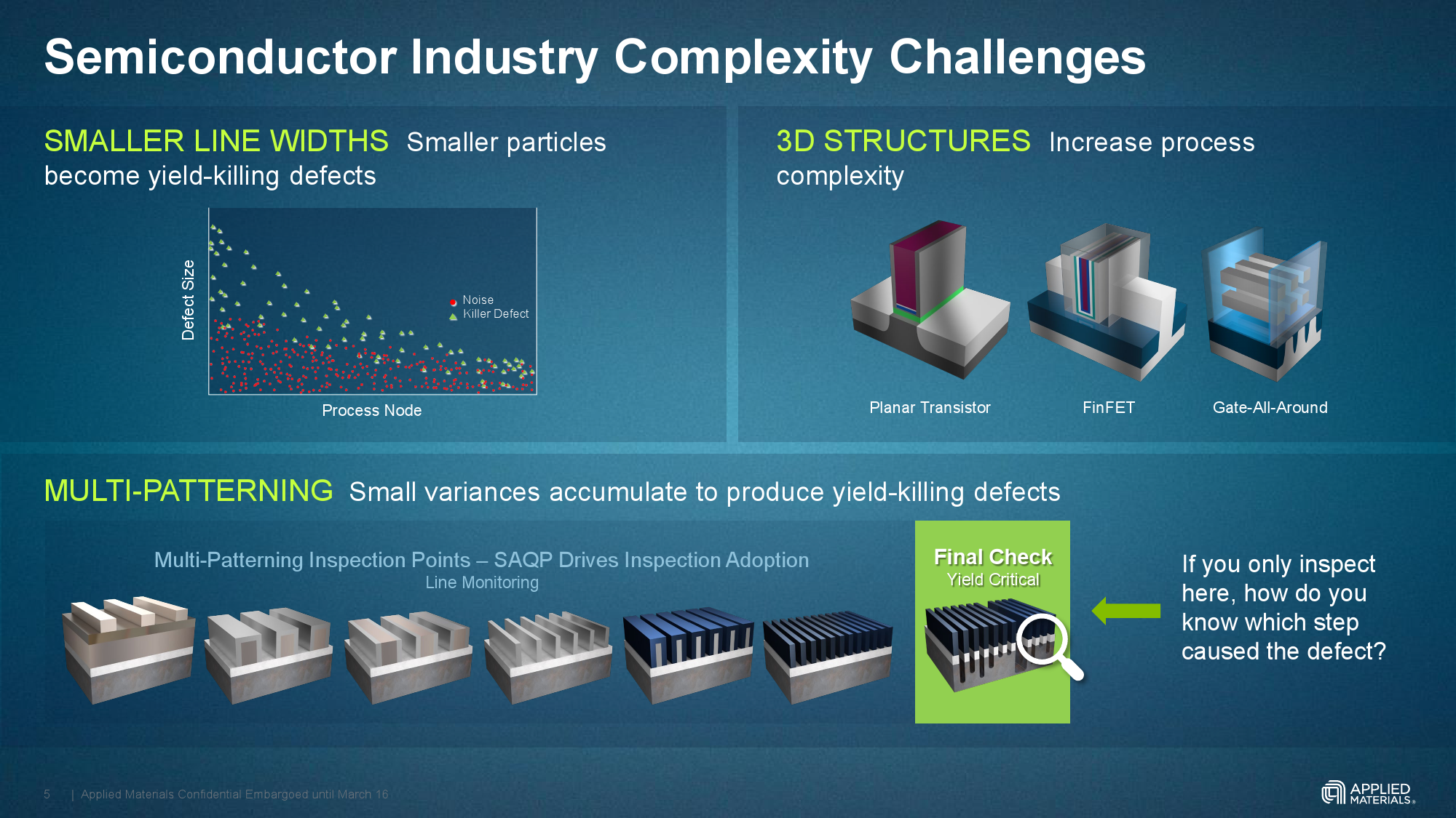
Meanwhile, small variances and line widths can end up as yield-killing defects if they multiply. Furthermore, if these tiny variances are detected late, all the process steps made after the variance was introduced are essentially wasted time and money. In fact, even late detection can be considered bad luck, as tracking down the root cause of a defect of an IC featuring FinFET transistors and made using multi patterning is extremely hard.
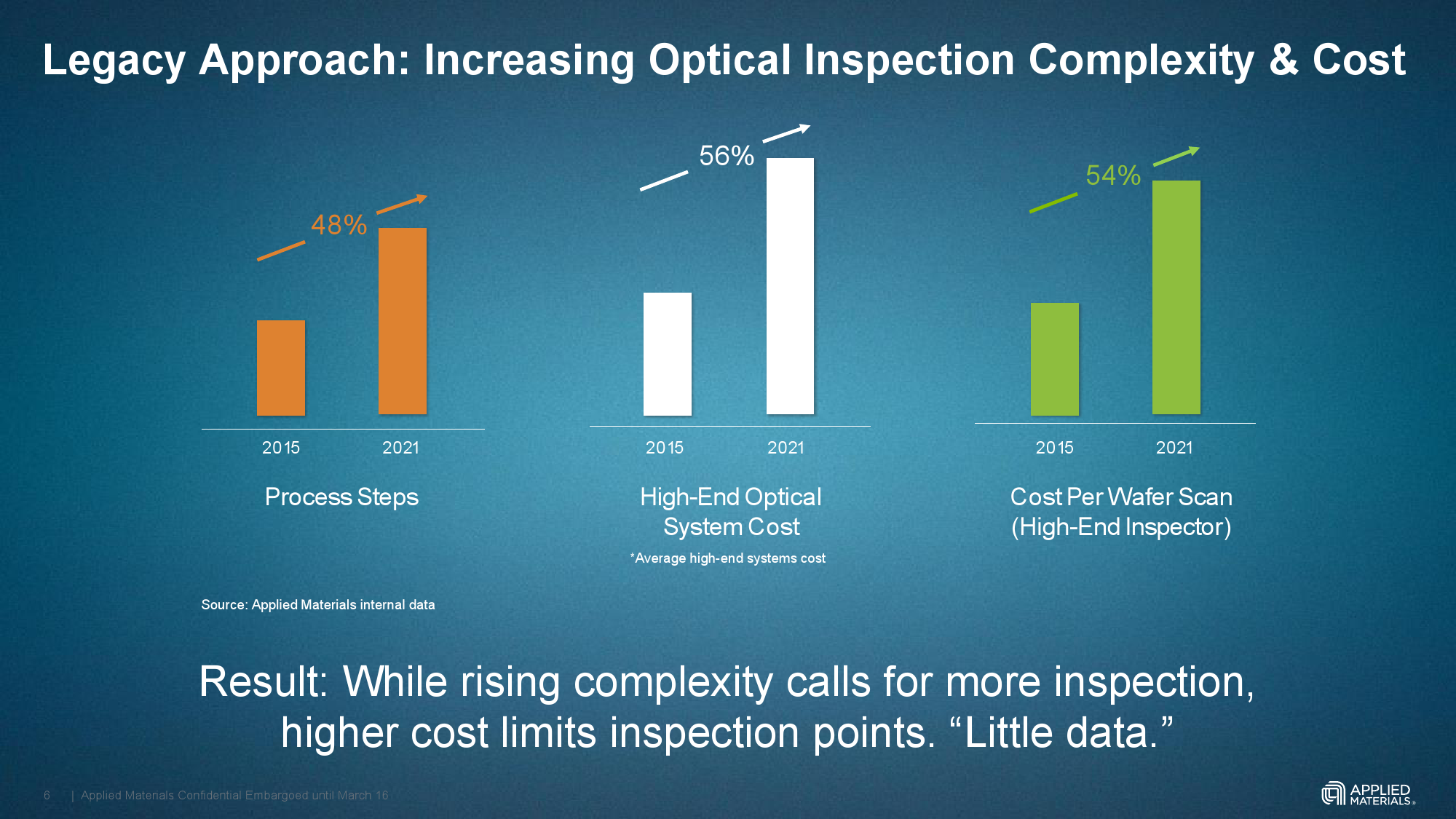
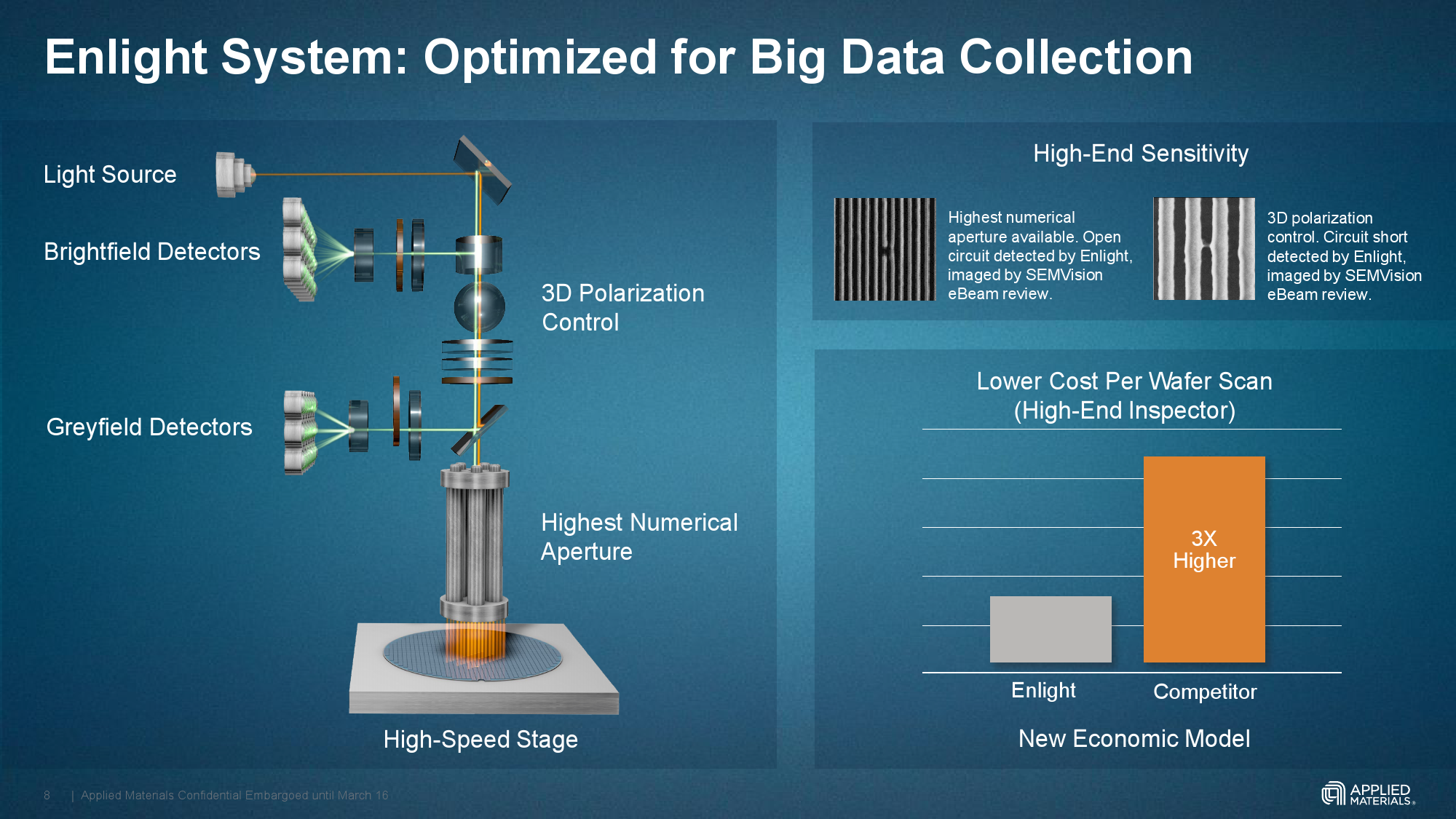
Just like scanners used to build chips, inspection tools have evolved significantly over the years. But they also have become more expensive, which increases cost per wafer scan. According to Applied Materials, the price tag on a high-end optical inspection system has increased by 56% in the last six years, which in turn has increased the cost per wafer scan by 54% in the same period.
As a result, the fab industry faces a catch-22. On the one hand, it needs to do more inspections (preferably after each process step) in order to speed up time to yield and make production more efficient. Furthermore, chipmakers are always performing continuous process improvements (CPI), to improve yields and reduce performance/power variations using statistical process control (SPI), which again involves additional inspections. But on the other hand, since there are so many process steps today and the inspection tools are so expensive, engineers have to limit inspection steps to keep their process control budgets from skyrocketing, which essentially stretches out the time to yield and while slowing down the CPI process.
Yet another problem faced by fab engineers is the amount of noise that is captured by modern optical inspection tools. At some point noise becomes indistinguishable from yield-killing defects, so engineers have to apply certain filtering models to reduce datasets they have to work with. Quite naturally, this reduces their ability to detect a defect early enough.
Using AI for Wafer Inspection
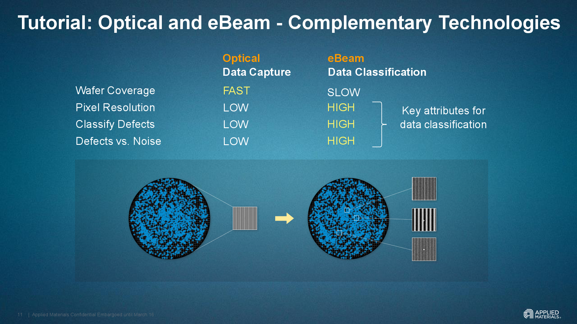
This brings us to Applied Materials' ExtractAI technology. As one of the world's largest production tool manufacturers, Applied Materials has their hand in a broad range of inspection tools, including optical inspection tools and e-beam review tools. So the company is looking to tap its expertise in the field to find a way to use both technologies to mitigate each tool's respect drawbacks – fast-but-resolution-limited optical inspection tools, and slow-but-detailed e-beam tools.
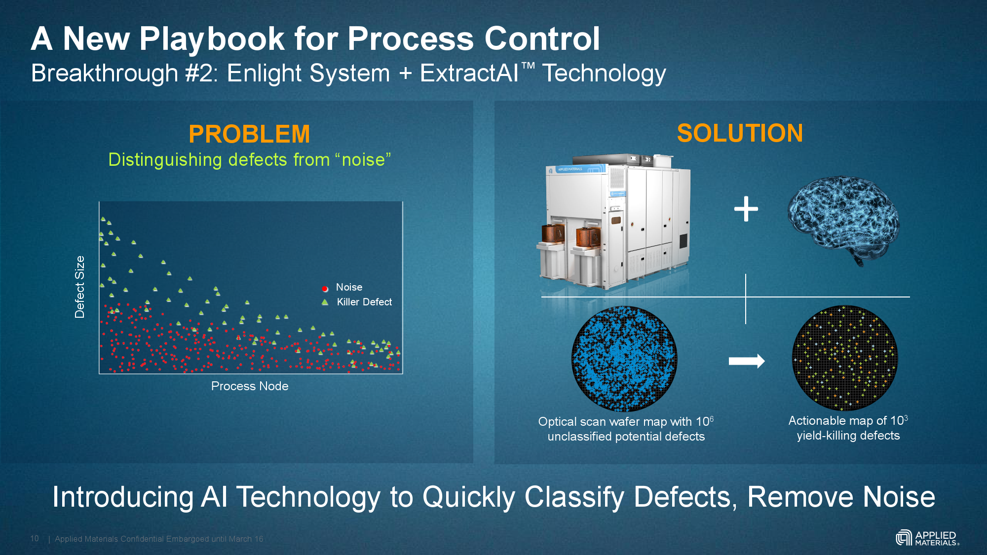
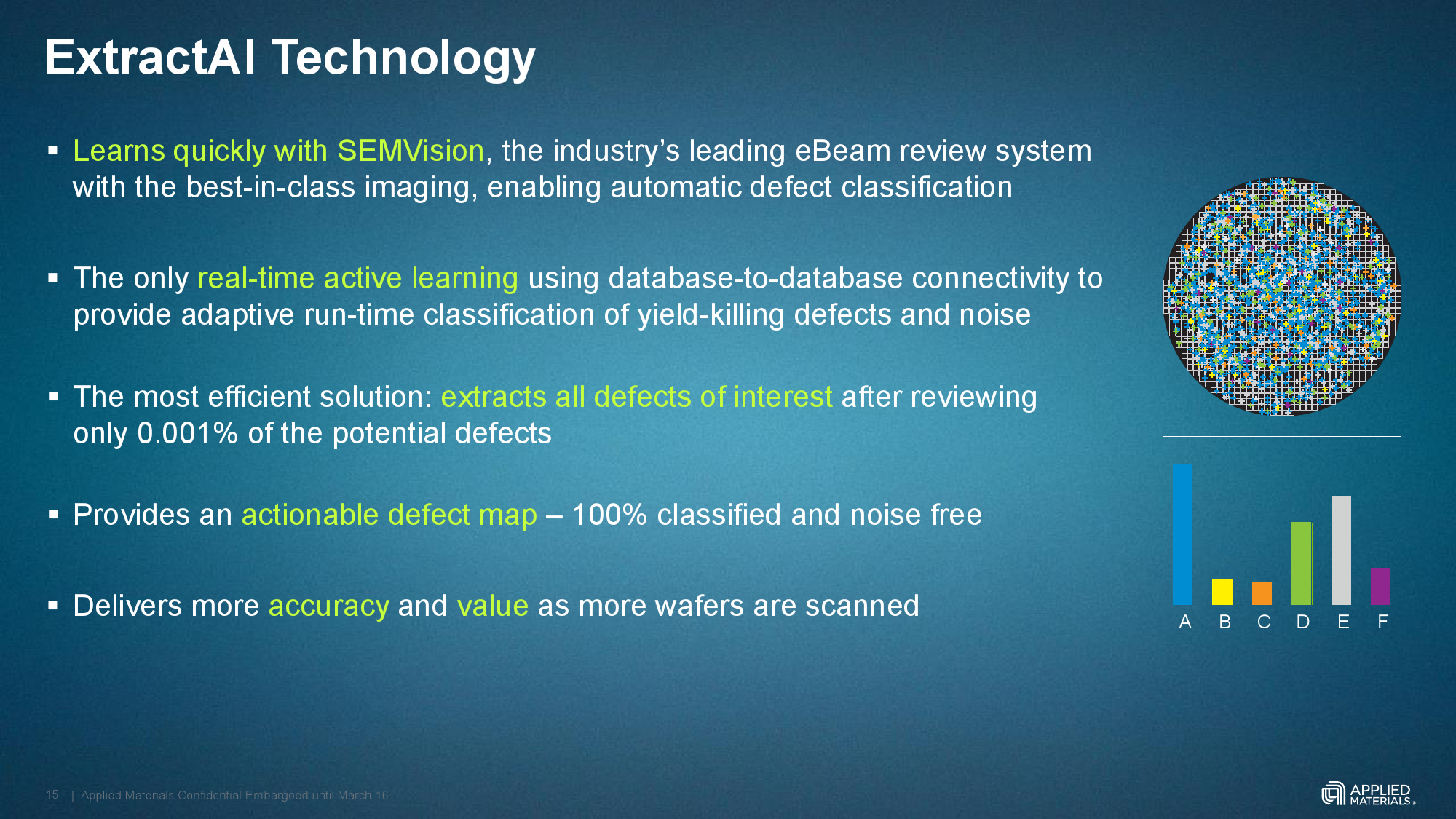
To that end, Applied Materials has combined its latest Enlight optical wafer inspection system with their new ExtractAI technology. The ExtractAI software essentially uses deep learning (AI) to try to better interpret the results of optical scanners, processing the optical data while using their SEMVision G6/G7 e-beam review system as a source of training and results verification.
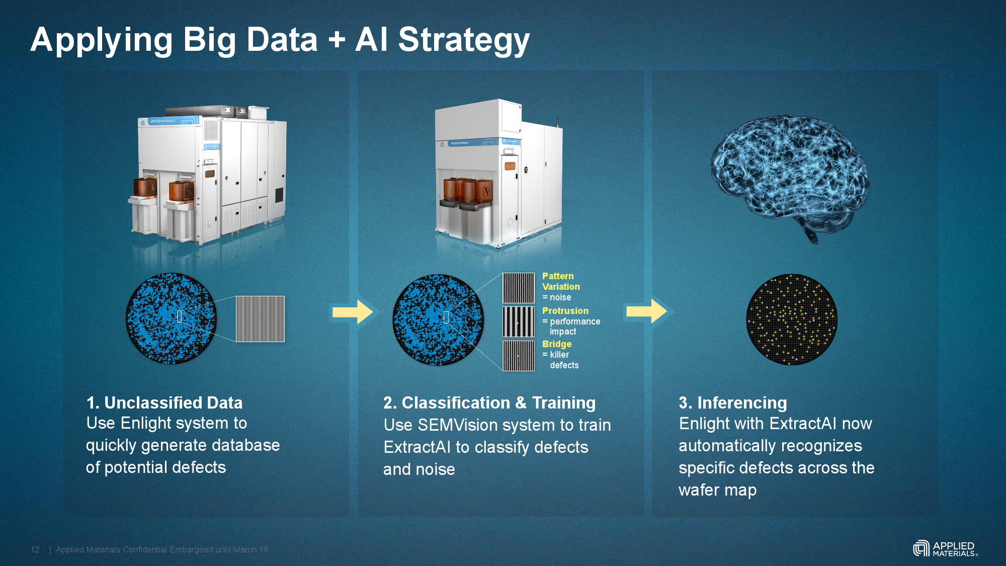
On paper, everything works pretty straightforward. An Enlight system captures a high-resolution image of a wafer and quickly generates database of potential defects. The wafer is then sent to a SEMVision G6/G7 e-beam review system that distinguishes defects from noise and classifies defects. Images and data captured by the Enlight and the SEMVision G6/G7 are then fed to the ExtractAI software to train it to automatically recognize specific yield-killing defects across the wafer map generated using the hardware systems and distinguish them from noise.
As a result, the scanning process takes considerably less time with future wafers of the same chip, as the systems already have an actionable wafer map with potential yield-killing defects and should know what to look for. Meanwhile, as the ExtractAI software gains more data from more wafers, the additional training should allow it to offer even more accuracy and performance. Especially as the resulting defect databases can be shared across a fab or even across the whole company.
Already at Work
As it usually happens with Applied Materials' announcements, their newest toolset is already installed at multiple fabs. According to the company, their Enlight optical inspection tool with ExtractAI technology is already in use at logic fabs in South Korea, Taiwan, and the U.S., all of whom are using it to improve the time to yield of their latest technologies.
"The additional data obtained by line monitoring enables me to accelerate and manage yields in a way that I could never afford to do before," said an unnamed customer of Applied in June 2020 (according to the company's presentation).
Applied Materials started development of the Enlight system with ExtractAI in 2016, with commercial shipments to logic producers beginning in Q1 2020. By the end of Q1 2021, cumulative sales of the inspection tool are expected to exceed $400 million. Applied's SEMVision e-beam inspection tools are also widely used by the industry (over 1,500 units have been installed since 1998), but only the SEMVision G6, G7 and their successors are compatible with the Enlight and ExtractAI.
Today, Applied Materials' Enlight optical inspection system with ExtractAI technology are being used by leading logic fabs (since there are not many of them, their names are not hard to guess). But as DRAM process technologies continue to get more complex, the company is expecting that manufacturers in other fab fields will adopt Applied's deep learning-driven toolset in the coming quarters and years as well.


11 Comments
View All Comments
Altuzza - Thursday, June 17, 2021 - link
Hi there! A few months ago, I was looking for the answer to the same question. I found this company https://axonim.com/ . They said that they are the best software development company. I trusted them, and yeah, actually, they are. They finished my project in a month, and now they are working on my 3rd project.