AMD 3rd Gen EPYC Milan Review: A Peak vs Per Core Performance Balance
by Dr. Ian Cutress & Andrei Frumusanu on March 15, 2021 11:00 AM ESTTopology, Memory Subsystem & Latency
For users who are already familiar with AMD’s newest Zen3 microarchitecture from our coverage of the new Ryzen 5000 consumer parts, they will remember that one big change the way configures their CPU topology is how the new CCX (Core Complex) is integrated within a CCD (Core Chiplet Die).
Previous generation Zen2 and prior designs of the Zen microarchitecture consisted of CCXs of four CPU cores, with a set amount of L3 cache shared between these four cores – 8MB in the original Zen iterations and 16MB in Zen2 variants. In Zen3, AMD has redesigned their L3 implementation to now support up to 8 physical cores in one core complex. Effectively, AMD is doubling the L3 and cores per CCX. The CCD in turn however instead of housing two CCXs, now only houses one, which effectively means that the total L3 and core count per core chiplet doesn’t change between the generations.
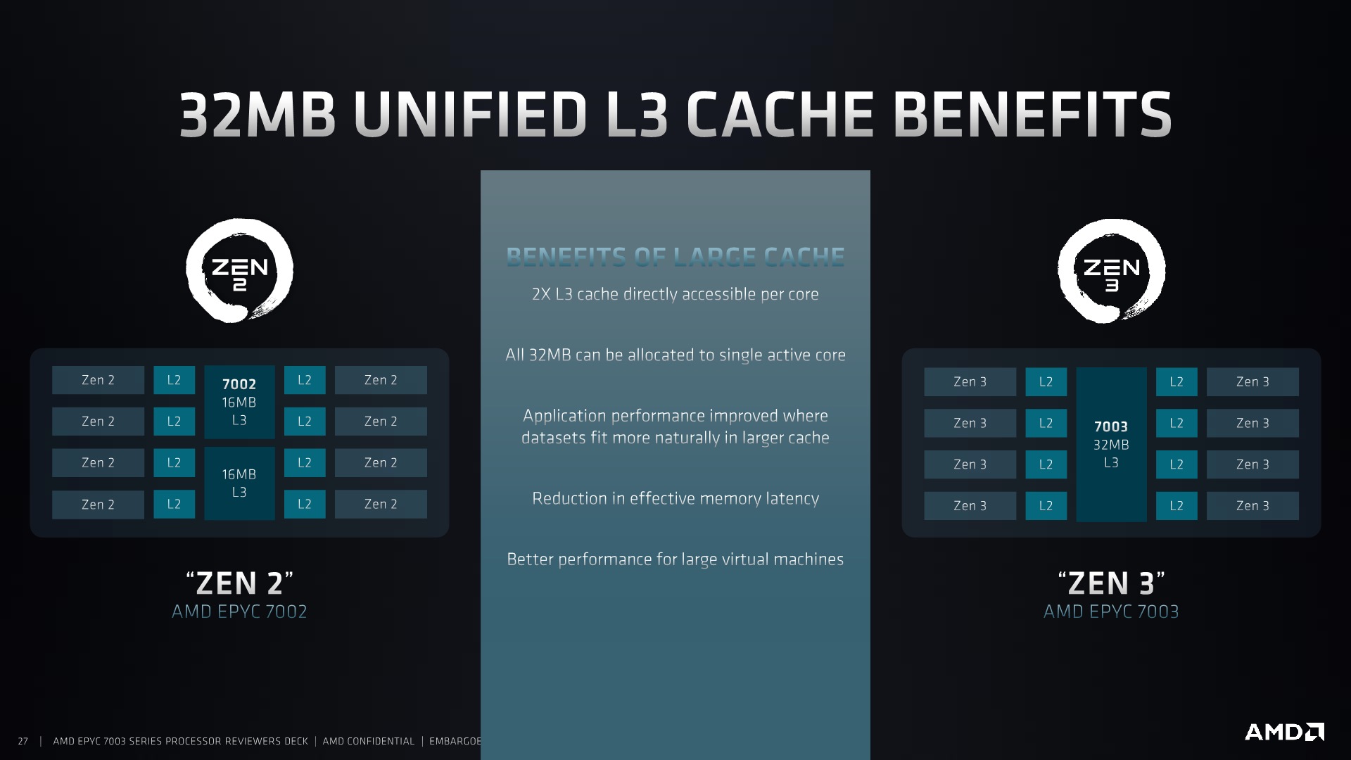
Benefits for the new arrangement is that this enlarges the L3 cache hierarchy from the view of a single CPU core, allowing each core to possibly make use of the full 32MB of cache. Furthermore, because the CCX is now 8 cores instead of 4 cores, inter-core access latencies to other cores can effectively be reduced when workloads are resident on the cores within that CCX. Previously, even if two cores were on the same physical die, but on different CCXs, communications between the two had to take place via external routing through the IOD (I/O Die) of the CPU package, incurring large access penalties. AMD here also makes an interesting argument for larger virtual machines which are bound to a single CCD across 8 cores, something which was previously not possible without performance hits due to spanning a VM across multiple CCXs.
We can test out the physical topology of the CPUs by running our inter-core synchronisation latency test. As a reminder, our inter-core bounce test consists of an initial main thread which allocates the synchronisation cache line on the core that the executable is spawned on – we try to fix this to the first NUMA node / CPU group of the first socket. This in turn spawns two ping-pong threads which bounce around based on the shared cache line, and we change the affinity of the threads across the system to test out the various core-to-core latencies. Because of the usage of a common shared cache line – usually how real software works; we’re essentially testing core-to-cacheline-to-core – an important distinction to make for some systems which have different cache line placement and cache coherency algorithms.

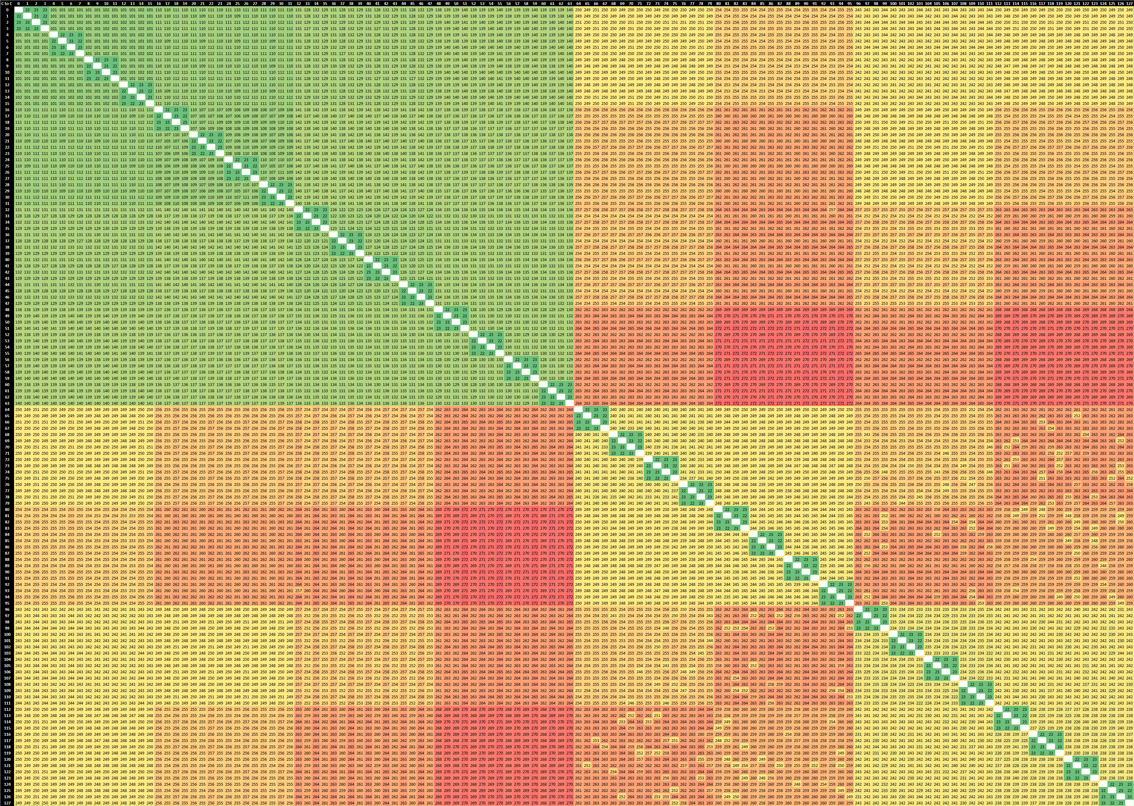
2-Socket AMD EPYC 7763 (Milan)
Right off the bat, what’s immediately visible in the new EPYC 7763 64-core Milan based part is that the CCXs have grown in size, now spanning 8 cores, with the corresponding lower latency results within that cache hierarchy. The result set here is limited to just the physical cores as otherwise the logical SMT siblings would have resulted in a 256 x 256 matrix for a 2-socket system.
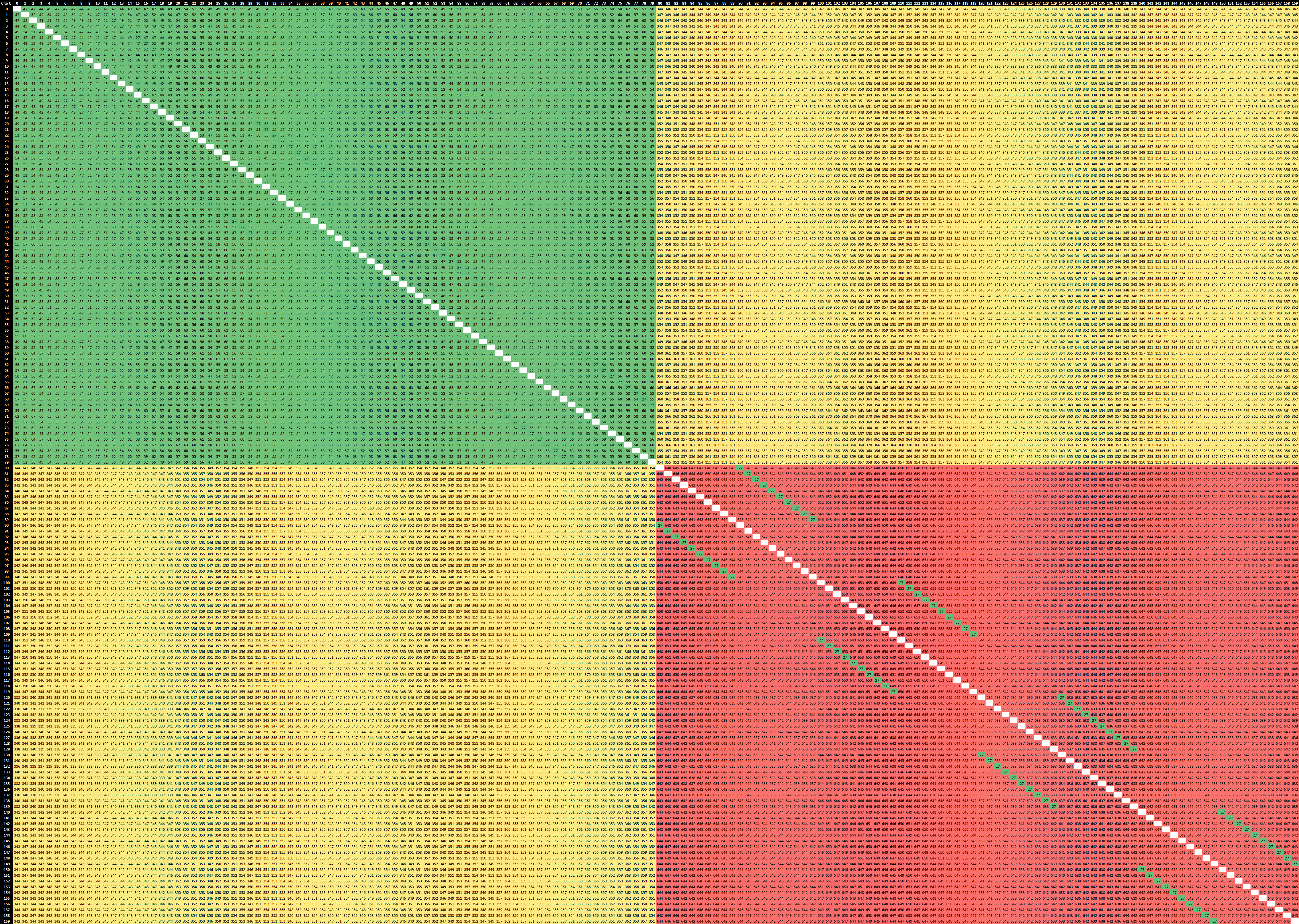
2-Socket AMD EPYC 7742 (Rome)
If we contrast the new Milan design to the Rome-based EPYC 7742, we’re seeing quite a few differences between the two generations. First of all, within the CCX/CCD, we’re not seeing that access latencies aren’t as uniform anymore. Previously we saw latencies at 22-23ns, whereas the new part now varies from 19 to 31ns, which is due to AMD’s doubling of the L3 which has seen a new internal topology between the 8 cache slices. It’s to be noted that the test here ran around 3400MHz between both generation parts.
AMD’s server IO die is divided into quadrants, each featuring two memory controllers and two connections to CCDs. Access latencies between two CCDs in a quadrant is lower than between two CCDs in different quadrants, and we can also see this in the results. The core-to-core latency within a quadrant this generation has improved from a worst-case 112ns to 99ns, about a 10ns improvement. Access to remote quadrants has been reduced from up to 142ns to up to 114ns, which is actually a 24% improvement, which is considerable.
What’s really interesting is that inter-socket latencies have also seen very notable reductions. Whereas the Rome part these went up to 272ns, the new Milan part reduces this down to 202ns, again a large 25% improvement between generations.
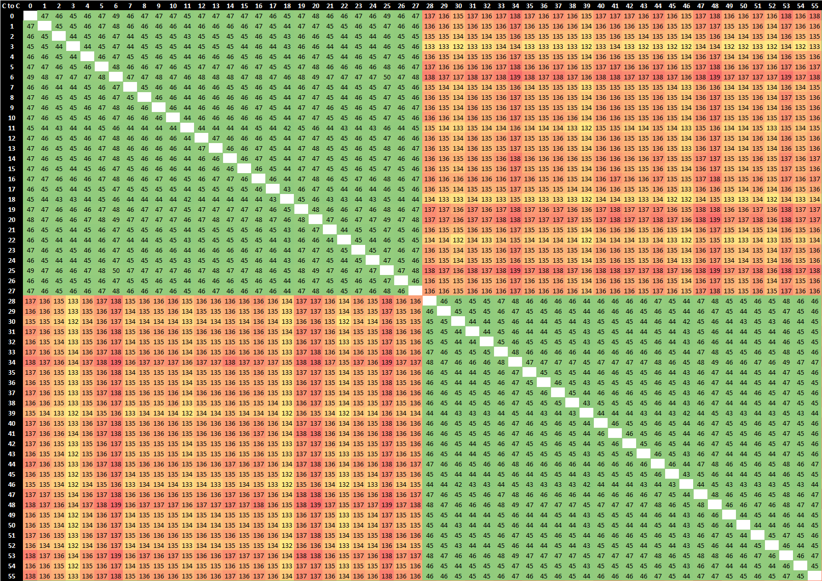
2-Socket Ampere Altra Q80-33 --------- 2-Socket Intel Xeon Platinum 8280
Compared to other competitors which use monolithic silicon designs, AMD lags behind in terms of core-to-core latencies within a single socket, although latencies within a CCX/CCD are more performant. Inter-socket latencies are superior to newcomers such as Ampere’s Altra, however lag behind Intel’s seemingly superior cache coherency protocol, particularly in scenarios where two cores of a same socket access a remote socket cache line, being able to locally copy/mirror it with native performance, something AMD currently is only able to do at a CCX/CCD level.
Memory Latency
Memory latency on Milan is interesting as AMD is now employing a new IOD design. Well – it’s not a completely new design from the previous generation Rome IOD, however it is a redesign with new features, with slightly more transistors and it is a new chip tape-out.
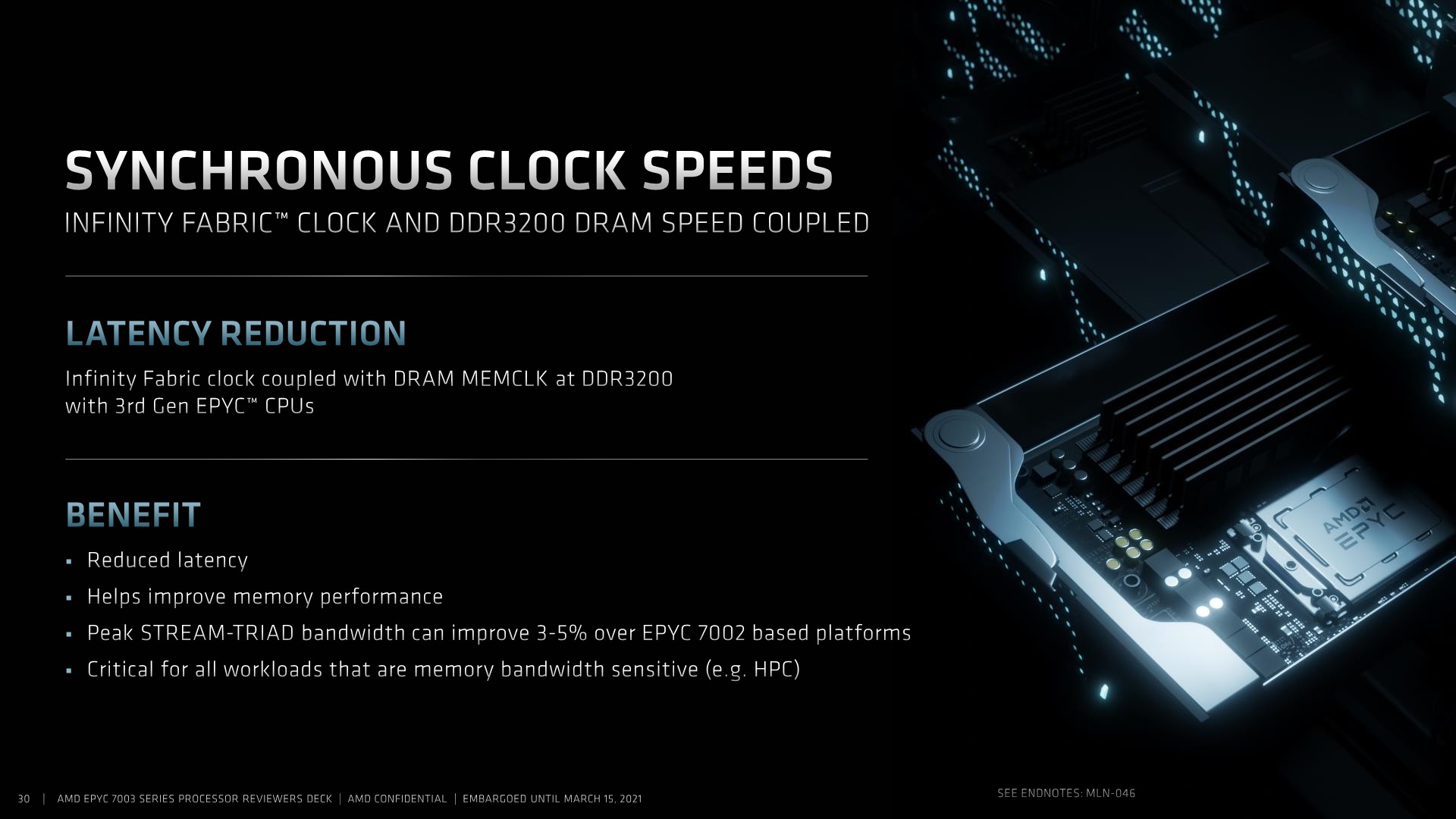
The biggest practical change of the new chip is that the internal Infinity Fabric clock is now coupled with the memory controller clocks / DRAM MEMCLK, at up to DDR3200. The much-improved inter-core latencies discussed above are likely direct result of this change, but it should also have larger impact on the memory latency of the new Milan chips.
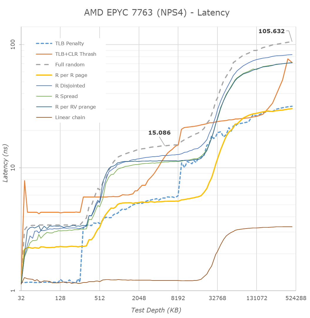
Starting off in NPS4 mode, a NUMA node in which a socket is divided into 4 non-uniform memory address spaces, representing the four physical quadrants of the IOD, each NUMA node and quadrant with the local 2 CCDs and 16 cores only have access to their local 2 memory channels.
Latencies here see a reduction from 118ns down to 105ns, which is a 11% improvement. The 13ns improvement should be a direct result of the new Milan part having to avoid asynchronous clock bridges between the Infinity Fabric and the memory controllers.
The latencies at the lower cache hierarchies within the new L3 and Zen3 cores looks pretty identical to what we’ve measured on the consumer Ryzen 5000 parts – with the only difference of course that the EPYC CPUs are running at lower frequencies.
What I’d say is interesting, is how the prefetchers behave compared to Rome. AMD this generation with Zen3 has changed things up quite a bit with newer generation prefetchers, including a new region-based prefetcher. On the Rome parts we saw that the more advanced prefetchers enabled/disabled themselves depending on access pattern depth. On Milan, this doesn’t seem to be the case, at least for some of our patterns.
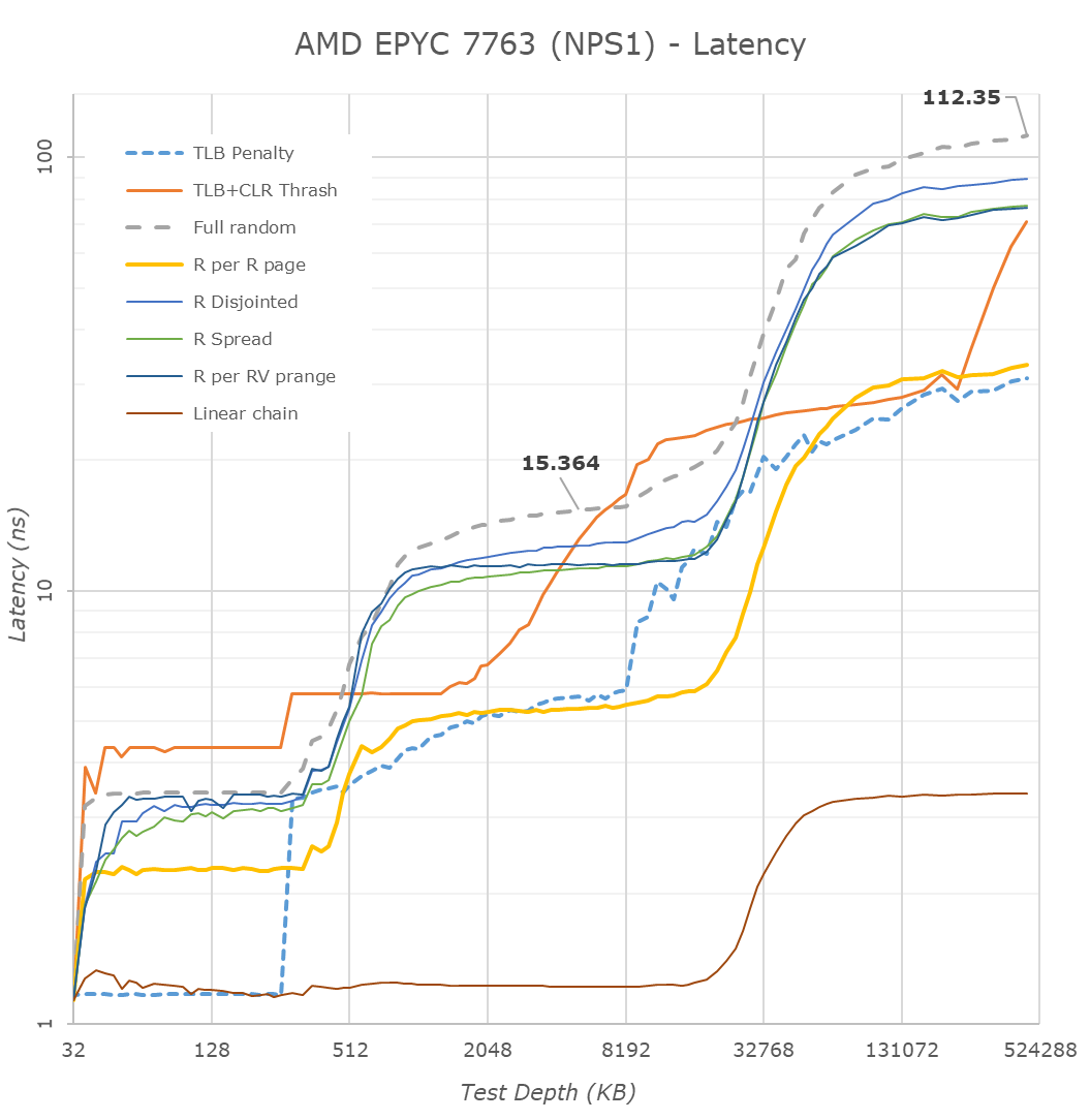
Although the best latencies are to be had in NPS4 mode, sometimes you want just a single large NUMA node with full access to the total memory of a single socket (AMD also offers NPS0 mode with interleaving memory across two sockets, but that’s beyond our scope here). Here, a single CPU will interleave memory accesses across all four quadrants and eight memory channels, but due to the physical design of the chip this naturally means the data has to travel longer distances, and thus latencies are expected to be worse than in NPS4 mode.
Surprisingly, the new 7763 Milan part is showing extremely large improvements in NPS1 mode – reducing latencies from 133ns down to 112ns, a 21ns reduction, representing a 15.8% improvement over the 7742 Rome part. Although naturally still not quite matching monolithic chip access latencies as seen from a Xeon or Altra system, it’s significantly better this generation.
Memory Bandwidth
For memory bandwidth, AMD had advertised a 3-5% improvement in STREAM-Triad compared to previous generation 7002 series CPUs, so let’s put that to the test.
We’re opting for a regularly compiled STREAM binary using GCC 10.2, and are avoiding the use of explicit non-temporal memory accesses as I do not consider them to be real-world for how most workloads behave. I had explained this rationale in our review of the Ampere Altra a few months ago.
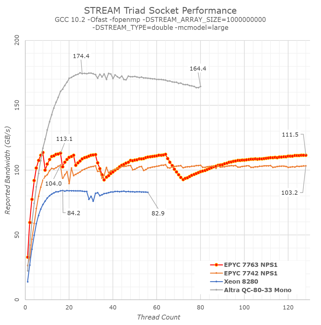
Also, instead of looking at a single test result figure, I charted the bandwidth curves of the system when scaling from 1 thread/core to the full 128 threads of the system.
In terms of peak memory bandwidth, we’re seeing that indeed the new Milan-based chip around 8% higher than the Rome-based predecessor, slightly above AMD’s marketed projections. AMD hadn’t clarified whether these were NPS1 or NPS4 figures, but we prefer using STREAM to measure bandwidth within a single memory node – scaling up to multiple nodes should normally be expected to simply be a multiple of the node.
What’s really interesting in the behaviour of the Milan system is the bandwidth scaling at lower thread/core counts. Here we’re seeing the new 7763 take the lead by considerable margins compared to the competition, and the Milan chip is able to actually reach its peak memory bandwidth with only 8 cores, whereas the Rome-based parts required 16 cores to reach this point. The cause of these excellent results is likely the much-improved load/store capabilities of the new Zen3 cores.
What’s odd here in the bandwidth curve, is the zig-zag pattern, with bandwidth sometimes regresses below earlier achieved peak figures. We’re placing threads with OMP_PLACES="cores" and OMP_PROC_BIND="spread", however this might still not be optimal in terms of spreading load symmetrically across all CCDs in the system.


120 Comments
View All Comments
Oxford Guy - Tuesday, April 6, 2021 - link
PSP, as far as I know.Linustechtips12#6900xt - Monday, March 15, 2021 - link
I understand that "zen" architecture is for x86 but with modifications could it be transplanted to the ARM instruction set, as i see it, it definitely could so the real question is when will the transition really start i think around the theoretical zen 5th gen or 6th gen, theres gonna be a lot of arm around here especially with apple. and yes it will defenitly start wiht servers it always does.Gomez Addams - Monday, March 15, 2021 - link
There are really two things at work : the instruction set of the processor and its topology. AMD has been improving both quite a bit. The instruction set enhancements won't transfer quite so well to ARM but the topology certainly can. Since ARM processors are much smaller, they could probably work in chiplets with possibly 32 cores in each or maybe 16 cores and 4-way SMT. That could make for a very impressive server processor. Four chiplets would give 64 cores and 256 threads. Yikes!rahvin - Monday, March 15, 2021 - link
So much wrong.mode_13h - Monday, March 15, 2021 - link
There are pieces of it that can be reused (on the same manufacturing node, at least), but making a truly-competitive ARM chip is probably going to involve some serious tinkering with the pipeline stages & architecture. And there are significant parts of an x86 chip that you'd have to throw out and redo, most notably the instruction decoder.In all, it's a different core that you're talking about. Not like CPU vs. GPU level of difference, but it's a lot more than just cosmetics.
coder543 - Monday, March 15, 2021 - link
"For this launch, both the 16-core F and 24-core F have the same TDP, so the only reason I can think of for AMD to have a higher price on the 16-core processor is that it only has 2 cores per chiplet active, rather than three? Perhaps it is easier to bin a processor with an even number of cores active."If I were to speculate, I would strongly guess that the actual reason is licensing. AMD knows that more people are going to want the 16 core CPUs in order to fit into certain brackets of software licensing, so AMD charges more for those to maximize profit and availability of the 16 core parts. For those customers, moving to a 24 core processor would probably mean paying *significantly* more for whatever software they're licensing.
SarahKerrigan - Monday, March 15, 2021 - link
Yep.Intel sold quad-core Xeon E7's for impressively high prices for a similar reason.
Mikewind Dale - Monday, March 15, 2021 - link
Why couldn't you run a 16 core software license on a 24 core CPU? I run a 4 core licensed version of Stata MP on an 8 core Ryzen just fine.Ithaqua - Monday, March 15, 2021 - link
Compliance and lawsuits.You have to pay for all the cores you use for some software.
Yes if you're only running 4 cores on your 8 core Ryzen then your fine but Stata MP is using all 8, there could be a lawsuit.
Now for you I'm sure they wouldn't care. For a larger firm with 10,000+ machines, then that's going to be a big lawsuit.
arashi - Wednesday, March 17, 2021 - link
Some licenses charge for ALL cores, regardless of how many cores you would actually be using.