Understanding the Cell Microprocessor
by Anand Lal Shimpi on March 17, 2005 12:05 AM EST- Posted in
- CPUs
Cell’s On-Die Memory Controller
For years, we’ve known that Rambus’ memory and interface technology is well ahead of the competition. The problem is that it has never been implemented well on a PC before. The Rambus brand received a fairly negative connotation during the early days of RDRAM on the PC, and things worsened even more for the company’s brand with the Rambus vs. the DDR world lawsuits.Rambus has had success in a lot of consumer electronics devices, such as HDTVs and the Playstation 2, so when Cell was announced to make heavy use of Rambus technologies, it wasn’t too surprising. As we’ve reported before, Rambus technology is used in about 90% of the signaling pins on Cell. The remaining 10% are mostly test pins, so basically, Rambus handles all data going in and out of the Cell processor. They do so in two ways:
First off, Cell includes an on-die dual channel XDR memory controller, each channel being 36-bits wide (32-bits with ECC). Cell’s XDR memory bus runs at 400MHz, but XDR memory transfers data at 8 times the memory bus clock - meaning that you get 3.2GHz data signaling rates. The end result is GPU-like memory bandwidth of 25.6GB/s. As we’ve mentioned in our coverage of this year’s Spring IDF, memory bandwidth requirements increase tremendously as you increase the number of processor cores - with 9 total in Cell, XDR is the perfect fit. Note that the GeForce 6800GT offers 32GB/s of memory bandwidth just to its GPU, so it would not be too surprising to see the Playstation 3’s GPU paired up with its own local memory as well as being able to share system memory and bandwidth.
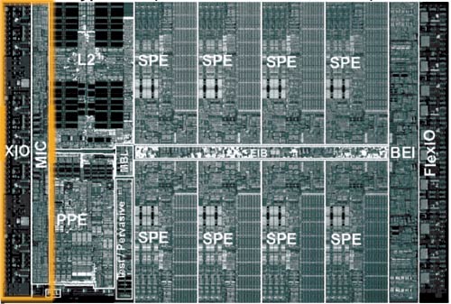
The block labeled MIC is the XDR memory controller, and the XIO block is the physical layer - all of the input receivers and output drivers are in the XIO block. Data pipelines are also present in the XIO block.
Cell’s On-Die FlexIO Interface
The other important I/O aspect of Cell is also controlled by Rambus - the FlexIO interface. Cell features two configurable FlexIO interfaces, each being 48-bits wide with 6.4GHz data signaling rates.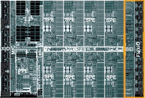
The BEI block is effectively the North Bridge interface, while the FlexIO block is the physical FlexIO layer.
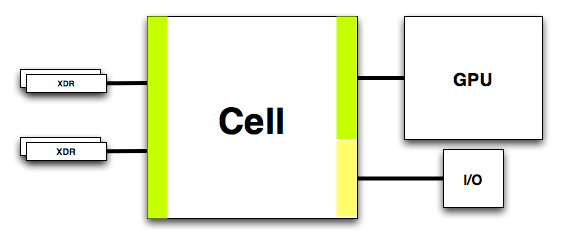
One potential implementation of Cell’s configurable FlexIO interface.
In Playstation 3, you can pretty much expect a good hunk of this bandwidth to be between NVIDIA’s GPU and the Cell processor, but it also can be used for some pretty heavy I/O interfaces.
One of the major requirements in any high performance game console is bandwidth, and thanks to Rambus, Cell has plenty of it.


70 Comments
View All Comments
Poser - Thursday, March 17, 2005 - link
There were moments while reading this article that I expected there to be a "Test Yourself" quiz at the end of the chapter ... er, article. Which isn't to say that articles like this are too textbookish, it's to say that they're wonderfully educational. And very, very cool for being so.I'm half joking when I say this (but only half) -- a real "test" at the end of the article would be fun. I could see if I really understood what I read, and even get to compare my score to the rest of the, uhm, class.
drinkmorejava - Thursday, March 17, 2005 - link
very nice, how long did it take to write that thing?Eug - Thursday, March 17, 2005 - link
#42,That's an interesting page, cuz everyone on OS X already knows that Word is slow on the Mac. It brings us back to the original statement that some ported software may be problematic performance-wise.
And the generic comment on the Mac side about Premiere is, well... use Final Cut Pro. :) Here is a test that seems a bit more useful, since it tests Cinema4D and After Effects, two apps that people use on the Mac and both of which are reasonably well optimized:
http://digitalvideoediting.com/articles/viewarticl...
That's a good point about the memory scaling though. The IMC with AMD's chips is a definite advantage. I'm sure the G5 970MP dual-core won't get an IMC either.
Anyways, as far as this article is concerned, the G5 is kinda irrelevant. The interesting part for Apple in Cell is the PPE unit. It's also interesting that Anand says the original SPE was supposed to be VMX/Altivec. But the current SPE is not Altivec so it's less applicable for Apple, at least in the near term.
It would be interesting to know how fast a dual-core 3 GHz PPE would be in general laptop-type code, and how much power it would put out.
MDme - Thursday, March 17, 2005 - link
#39, 40, 41http://www.pcworld.com/news/article/0,aid,112749,p...
remember that the athlon 64 chips scale better at higher clock speeds due to the mem controller scaling as well.
Eug - Thursday, March 17, 2005 - link
Well, one example is Cinebench 2003:The dual G5 2.0 GHz is about the same speed as a dual 0pteron 246 2.0 GHz, with a score at around 500ish.
http://www.aceshardware.com/read.jsp?id=60000284
BTW, a dual G5 2.5 GHz scores 633.
suryad - Thursday, March 17, 2005 - link
Hmm that is interesting what you say Eug. I see your point do you have any links on straight comparos between an FX and a top of the line Mac? Or from personal experience folding and such...Eug - Thursday, March 17, 2005 - link
#38. It's a mistake to say an AMD FX 55 smokes a dual G5 2.5. For instance, if you like scientific dual-threaded stuff, the G5 does very well. However, the AMD FX 55 IS faster than a single G5 2.5. It's got a slight edge clock-for-clock, and it's clocked slightly higher too.The real problem is when you have stuff built for x86 ported over to PPC. It just isn't great on the Mac side performance-wise in that situation. And Macs aren't tweaked for gaming either. The AMD is going to smoke the Mac in Doom 3 of course.
I think with the performance advantage of the Opteron, I'd put a single G5 2.5 in the range of performance of a single Opteron 2.2-2.4 GHz, depending on the app. The real interesting part though will be the coming quarter, when the new G5s are released. They should get a significant clock speed bump (20%?) and information on dual-core G5s are already out there (like with AMD and their dual-core Athlons). They also get a cache boost. Right now they only have 512 KB, but are expected to get 1 MB L2.
suryad - Thursday, March 17, 2005 - link
Well scrotemaninov I am not disputing that the POWER architecture by IBM is brilliantly done. IBM is definitely one of those companies churning out brilliant and elegant technology always in the background.But my problem with the POWER technology is from what I understand very limitedly, is that the POWER processors in the Mac machines are a derivative of that architecture right? Why the heck are they so damn slow then?
I mean you can buy an AMD FX 55 based on the crappy legacy x86 arch and it smokes the dual 2.5 GHz Macs easily!! Is it cause of the OS? Because so far from what I have seen, if the Macs are any indication of the performance capabilities of the POWER architecture, the Cell will not be a big hit.
I did read though at www.aceshardware.com benchmark reviews of the POWER5 architecture with some insane number of cores if I recall correctly and the benchmarks were of the charts. They are definitely not what the Macs have installed in them...
scrotemaninov - Thursday, March 17, 2005 - link
#35: different approaches to solving the same problem.Intel came up with x86 a long time ago and it's complete rubbish but they maintain it for backwards compatibility (here's an argument for Open Source Software if ever there was one...). They have huge amounts of logic to effectively translate x86 into RISC instructions - look at the L1I Trace Cache in the P4 for example.
IBM aren't bound by the same constraints - their PowerPC ISA is really quite nice and so there's no where near the same amount of pain suffered trying to deal with the same problem. It does seem however, that IBM are almost at the point that Intel want to be in 10 years time...
Verdant - Thursday, March 17, 2005 - link
here is a question...it mentions (or alludes) in the article that having no cache means that knowing exactly when an instruction would be executed is possible, is the memory interface therefore a strict "real time system" ?