Understanding the Cell Microprocessor
by Anand Lal Shimpi on March 17, 2005 12:05 AM EST- Posted in
- CPUs
Cell’s On-Die Memory Controller
For years, we’ve known that Rambus’ memory and interface technology is well ahead of the competition. The problem is that it has never been implemented well on a PC before. The Rambus brand received a fairly negative connotation during the early days of RDRAM on the PC, and things worsened even more for the company’s brand with the Rambus vs. the DDR world lawsuits.Rambus has had success in a lot of consumer electronics devices, such as HDTVs and the Playstation 2, so when Cell was announced to make heavy use of Rambus technologies, it wasn’t too surprising. As we’ve reported before, Rambus technology is used in about 90% of the signaling pins on Cell. The remaining 10% are mostly test pins, so basically, Rambus handles all data going in and out of the Cell processor. They do so in two ways:
First off, Cell includes an on-die dual channel XDR memory controller, each channel being 36-bits wide (32-bits with ECC). Cell’s XDR memory bus runs at 400MHz, but XDR memory transfers data at 8 times the memory bus clock - meaning that you get 3.2GHz data signaling rates. The end result is GPU-like memory bandwidth of 25.6GB/s. As we’ve mentioned in our coverage of this year’s Spring IDF, memory bandwidth requirements increase tremendously as you increase the number of processor cores - with 9 total in Cell, XDR is the perfect fit. Note that the GeForce 6800GT offers 32GB/s of memory bandwidth just to its GPU, so it would not be too surprising to see the Playstation 3’s GPU paired up with its own local memory as well as being able to share system memory and bandwidth.
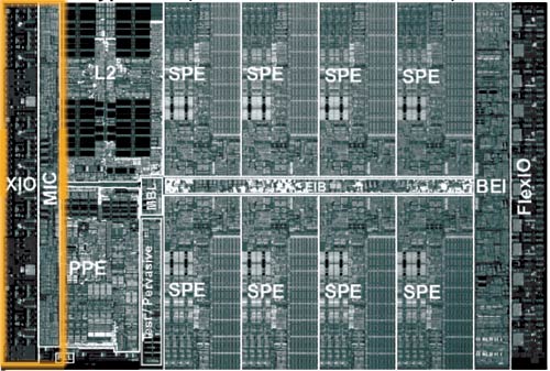
The block labeled MIC is the XDR memory controller, and the XIO block is the physical layer - all of the input receivers and output drivers are in the XIO block. Data pipelines are also present in the XIO block.
Cell’s On-Die FlexIO Interface
The other important I/O aspect of Cell is also controlled by Rambus - the FlexIO interface. Cell features two configurable FlexIO interfaces, each being 48-bits wide with 6.4GHz data signaling rates.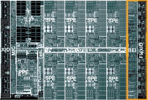
The BEI block is effectively the North Bridge interface, while the FlexIO block is the physical FlexIO layer.
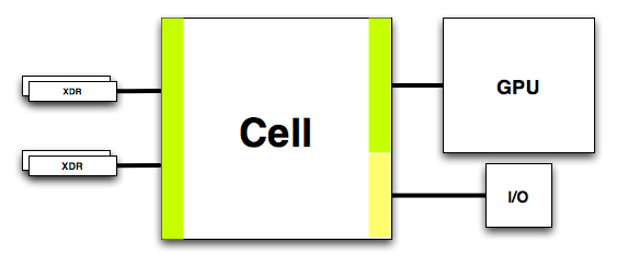
One potential implementation of Cell’s configurable FlexIO interface.
In Playstation 3, you can pretty much expect a good hunk of this bandwidth to be between NVIDIA’s GPU and the Cell processor, but it also can be used for some pretty heavy I/O interfaces.
One of the major requirements in any high performance game console is bandwidth, and thanks to Rambus, Cell has plenty of it.


70 Comments
View All Comments
Houdani - Friday, March 18, 2005 - link
I think I missed something fundamental.Can the SPEs be addressed directly by software, or do they have to be fed all of their instructions by the PPE?
If they DO have to be fed be the PPE, I fail to see how the PPE can possibly feed them enough to keep them all working concurrently.
Someone throw me a bone here.
suryad - Friday, March 18, 2005 - link
I thought the G5 was a POWER5 proc. But I could of course be wrong. All I can say is the Cell definitely intriguing as it may be will have a rough road ahead of it and I am quite surprised that these large corporations invested so much in it, cutting edge though it might be. And as for the current forseeable future, I think when multi-core FX processors from AMD comes out, I do not believe there will be anything more devastating than that. Especially once they hit the 3 Ghz barrier with multi-cores enabled and faster DDR2-3 or even RAMBUS memory capabilities.tipoo - Thursday, December 3, 2015 - link
No, G5 was 970 based.Questar - Friday, March 18, 2005 - link
#50,Yes the G5 is a POWER4 derivitive.
Since you were wrong on that, don't think that you know what is significant about the design of POWER5. There were major architechture changes made to the processor.
fitten - Friday, March 18, 2005 - link
The only things new about Cell is its target market and being a single chip. The article mentions the TI DSP chip, but there were other similar architectures as well. One example that I'm familiar with is the MAP1310 board by CSPI. Back then, processes weren't good enough to put all the cores on a single chip but the basic architecture is the same - a PPC core to do the 'normal' stuff and two quad-core DSPs (SHARC) to do the 'work'. This board wasn't successful because it was considered too hard to program to get the performance it promised.... and this opinion is from people who live/breathe real-time systems and multiprocessing codes.The only thing new about Cell is that a) it's all on one chip now and b) the target market is a general marketplace and not a niche.
scrotemaninov - Friday, March 18, 2005 - link
#48. OK, I was under the impression that the G5 was based on the POWER5. You're saying it's based on the POWER4 instead?And the POWER4 and POWER5 aren't really "completely different chips" in the same way that the P4 and P3 are different chips, or in the way that the P4 and the Opteron are different chips. I can give you a list of the differences if you want. Start at http://www.elet.polimi.it/upload/sami/architetture...
The POWER5 is designed to not only be completely compatible with the POWER4 but to also to support all the optimisations from the POWER4. The only things of significance they've done is a) move the L3 cache controller on chip; b) change the various branch predictors to bimodal instead of 1-bit; c) increase the associativity and size of the caches.
Anyway, this is going off topic now...
Jacmert - Friday, March 18, 2005 - link
Rofl. Computer engineering and VLSI design. Gotta love those NMOS/PMOS transistor circuits.I never thought that I'd see stuff from my textbook explained on anandtech.com
saratoga - Friday, March 18, 2005 - link
"#38. You're right that the G5 is a derivative of the POWER5. The POWER5 is dual core, each core with 2way SMT giving a total of 4 'visible' cpus to the OS. The G5 is simply a single core version of the same thing."Err no its not. POWER4 != POWER5. Hence the different names ;)
They're completely different chips.
"Well scrotemaninov I am not disputing that the POWER architecture by IBM is brilliantly done. IBM is definitely one of those companies churning out brilliant and elegant technology always in the background.
But my problem with the POWER technology is from what I understand very limitedly, is that the POWER processors in the Mac machines are a derivative of that architecture right? Why the heck are they so damn slow then?
I mean you can buy an AMD FX 55 based on the crappy legacy x86 arch and it smokes the dual 2.5 GHz Macs easily!! Is it cause of the OS? Because so far from what I have seen, if the Macs are any indication of the performance capabilities of the POWER architecture, the Cell will not be a big hit.
I did read though at www.aceshardware.com benchmark reviews of the POWER5 architecture with some insane number of cores if I recall correctly and the benchmarks were of the charts. They are definitely not what the Macs have installed in them..."
There are slow memeory systems and then theres the one used on the G5. I've heard that you can put 8 Opterons together and still get average access times across all 8 cores that are better then a single G5. Thats probably a good part of the reason the G5 was so much slower then many people thought it would be. The rest is mainly IBM's trouble making them, and their inability to ramp clock speed like they planned on.
scrotemaninov - Friday, March 18, 2005 - link
#38. You're right that the G5 is a derivative of the POWER5. The POWER5 is dual core, each core with 2way SMT giving a total of 4 'visible' cpus to the OS. The G5 is simply a single core version of the same thing.As for the performance, Opteron is pretty much unbeatable for integer-bound applications. Itanium2 is unbeatable for FP applications. POWER5 is somewhere in the middle.
Most desktop applications are going to be integer bound. So it's not at all surprising that you find the G5 'slow' in that respect in comparison to the FX55. Plus, and this is the whole problem with the CELL, there's no point putting dual CPUs in there unless you can utilise them properly. If you have one process going flat out trying to run a heavy application and it's single threaded then you're only using about 1/4 of the CPUs you've bought for that application (for a dual G5 2.5), whereas the Opterons and FX55 stuff is more designed around quick, single threaded applications.
dmens - Friday, March 18, 2005 - link
psuedo-pmos wtf? That's domino logic, it's been around forever, and it's definitely not efficient in terms of power. Oh, and it takes forever to verify timing.