Understanding the Cell Microprocessor
by Anand Lal Shimpi on March 17, 2005 12:05 AM EST- Posted in
- CPUs
High Level Overview of Cell
Cell is just as much of a multi-core processor as the upcoming multi-core CPUs from AMD and Intel, the only difference being that Cell's architecture doesn't have an entirely homogeneous set of cores.Cell's Execution Cores
The Cell architecture debuted in a configuration of 9 independent cores: one PowerPC Processing Element (PPE) and eight Synergistic Processing Elements (SPEs). The PPE and SPEs are obviously different, but all eight SPEs are identical to one another.The PPE is IBM's major contribution to the Cell project; it also appears to be very similar to the core being used in the next Xbox console.
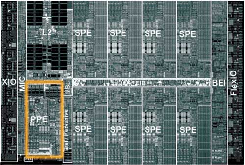
The PPE features a 64KB L1 cache and a 512KB L2 cache and features SMT, similar to Intel's Hyper Threading. The PPE features a strictly in-order core, which the desktop x86 market hasn't seen since the death of the original Pentium (the Pentium Pro brought out-of-order execution to the x86 market), so the move for an in-order core is an interesting one. The PPE is also only a 2-issue core, meaning that, at best, it can execute two instructions simultaneously. For comparison, the Athlon 64 is a 3-issue core, so immediately, you get the sense that the PPE is a much simpler core than anything that we have on the desktop. IBM's VMX instruction set (aka Altivec) is also supported by the PPE. Much like the rest of the Cell processor, the PPE is designed to run at very high clock speeds.
There's not much that's impressive about the PPE, other than it's a small, fast, efficient core. Put up against a Pentium 4 or an Athlon 64, the PPE would lose undoubtedly, but the PPE's architecture is one answer to a shift in the performance paradigm. Performance in business/office applications requires a very powerful, very fast general purpose microprocessor, but performance in a game console, for example, does not. The original Xbox used a modified Intel Celeron processor running at 733MHz, while the fastest desktops had 2.0GHz Pentium 4s and 1.60GHz Athlon XPs. Given that the first implementation of Cell is supposed to be Sony's Playstation 3, the simplicity of the PPE is not surprising. Should Cell ever make its way into a PC, the PPE would definitely have to be beefed up, or at least paired with multiple other PPEs.
The majority of the Cell's die is composed of the eight Synergistic Processing Elements (SPEs). If you consider the PPE to be a general purpose microprocessor, think of the SPEs as general purpose processors with a slightly more specific focus.
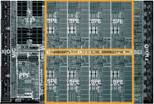
The SPEs have no branch predictor, meaning that they rely solely on software branch prediction. There are ways that the compiler can avoid branches, and the SPE architecture lends itself very well to things like loop unrolling. Any elementary programmer is familiar with a loop, where one or more lines of code is repeated until a certain condition is met. The checking of that condition (e.g. i < 100) often results in a branch, so one way of removing that branch is simply to unroll the loop. If you have a statement in a loop that is supposed to execute 100 times, you could either keep it in the loop and execute it that way, or you could remove the loop and simply copy the statement 100 times. The end result is the same - the only difference is that in one case, you have a branch condition while the other case results in more lines of code to execute.
The problem with loop unrolling is that you need a large number of registers to unroll some loops, which is one reason that each SPE has 128 registers. Originally, the SPEs were supposed to use the VMX (Altivec) ISA, but because of a need for more than 32 architectural registers, the SPEs implemented a new ISA with support for 128 registers.
Each SPE is only capable of issuing two instructions per clock, meaning that at best, each SPE can execute two instructions at the same time. The issue width of a microprocessor can determine a big part of how large the microprocessor will be; for example, the Itanium 2 is a 6-issue core, so being a 2-issue core makes each SPE significantly smaller than most general purpose microprocessors.
In the end, what we see with the SPEs is that they sacrifice some of the normal tricks to improve ILP in favor of being able to cram more SPEs onto a single die, effectively sacrificing some ILP for greater TLP. Given the direction that the industry is headed, a move to a very TLP centric design makes a lot of sense, but at the same time, it will be quite dependent on developers adhering to very specific development models.
Clearly, the architects of Cell saw the SPEs as being used to run a highly parallelizable workload, and as Derek Wilson mentioned in his article about AGEIA's PhysX PPU:
"One of the properties of graphics that made the feature a good fit for a specialized processor inside a PC is the fact that the task is infinitely parallelizable. Hundreds of thousands, and even millions of pixels, need to be processed every frame. The more detailed a rendering needs to be, the more parallel the task becomes. The same is true with physics. As with the visual world, the physical world is continuous rather than discrete. The more processing power we have, the more things we can simulate at once, and the more realistically we can approximate the real world."
With NVIDIA supplying some form of a GPU for Playstation 3, Cell's array of SPEs have one definite purpose in a gaming console - physics and AI processing. Many have argued that the array of SPEs seems capable of taking over the pixel processing workload of a GPU, but for a high performance console, that's not much of an option. The SPE array could offer better CPU-based 3D rendering, but it would be a tough sell (no pun intended) for this array of SPEs to be the end of dedicated GPU hardware.


70 Comments
View All Comments
Houdani - Friday, March 18, 2005 - link
I think I missed something fundamental.Can the SPEs be addressed directly by software, or do they have to be fed all of their instructions by the PPE?
If they DO have to be fed be the PPE, I fail to see how the PPE can possibly feed them enough to keep them all working concurrently.
Someone throw me a bone here.
suryad - Friday, March 18, 2005 - link
I thought the G5 was a POWER5 proc. But I could of course be wrong. All I can say is the Cell definitely intriguing as it may be will have a rough road ahead of it and I am quite surprised that these large corporations invested so much in it, cutting edge though it might be. And as for the current forseeable future, I think when multi-core FX processors from AMD comes out, I do not believe there will be anything more devastating than that. Especially once they hit the 3 Ghz barrier with multi-cores enabled and faster DDR2-3 or even RAMBUS memory capabilities.tipoo - Thursday, December 3, 2015 - link
No, G5 was 970 based.Questar - Friday, March 18, 2005 - link
#50,Yes the G5 is a POWER4 derivitive.
Since you were wrong on that, don't think that you know what is significant about the design of POWER5. There were major architechture changes made to the processor.
fitten - Friday, March 18, 2005 - link
The only things new about Cell is its target market and being a single chip. The article mentions the TI DSP chip, but there were other similar architectures as well. One example that I'm familiar with is the MAP1310 board by CSPI. Back then, processes weren't good enough to put all the cores on a single chip but the basic architecture is the same - a PPC core to do the 'normal' stuff and two quad-core DSPs (SHARC) to do the 'work'. This board wasn't successful because it was considered too hard to program to get the performance it promised.... and this opinion is from people who live/breathe real-time systems and multiprocessing codes.The only thing new about Cell is that a) it's all on one chip now and b) the target market is a general marketplace and not a niche.
scrotemaninov - Friday, March 18, 2005 - link
#48. OK, I was under the impression that the G5 was based on the POWER5. You're saying it's based on the POWER4 instead?And the POWER4 and POWER5 aren't really "completely different chips" in the same way that the P4 and P3 are different chips, or in the way that the P4 and the Opteron are different chips. I can give you a list of the differences if you want. Start at http://www.elet.polimi.it/upload/sami/architetture...
The POWER5 is designed to not only be completely compatible with the POWER4 but to also to support all the optimisations from the POWER4. The only things of significance they've done is a) move the L3 cache controller on chip; b) change the various branch predictors to bimodal instead of 1-bit; c) increase the associativity and size of the caches.
Anyway, this is going off topic now...
Jacmert - Friday, March 18, 2005 - link
Rofl. Computer engineering and VLSI design. Gotta love those NMOS/PMOS transistor circuits.I never thought that I'd see stuff from my textbook explained on anandtech.com
saratoga - Friday, March 18, 2005 - link
"#38. You're right that the G5 is a derivative of the POWER5. The POWER5 is dual core, each core with 2way SMT giving a total of 4 'visible' cpus to the OS. The G5 is simply a single core version of the same thing."Err no its not. POWER4 != POWER5. Hence the different names ;)
They're completely different chips.
"Well scrotemaninov I am not disputing that the POWER architecture by IBM is brilliantly done. IBM is definitely one of those companies churning out brilliant and elegant technology always in the background.
But my problem with the POWER technology is from what I understand very limitedly, is that the POWER processors in the Mac machines are a derivative of that architecture right? Why the heck are they so damn slow then?
I mean you can buy an AMD FX 55 based on the crappy legacy x86 arch and it smokes the dual 2.5 GHz Macs easily!! Is it cause of the OS? Because so far from what I have seen, if the Macs are any indication of the performance capabilities of the POWER architecture, the Cell will not be a big hit.
I did read though at www.aceshardware.com benchmark reviews of the POWER5 architecture with some insane number of cores if I recall correctly and the benchmarks were of the charts. They are definitely not what the Macs have installed in them..."
There are slow memeory systems and then theres the one used on the G5. I've heard that you can put 8 Opterons together and still get average access times across all 8 cores that are better then a single G5. Thats probably a good part of the reason the G5 was so much slower then many people thought it would be. The rest is mainly IBM's trouble making them, and their inability to ramp clock speed like they planned on.
scrotemaninov - Friday, March 18, 2005 - link
#38. You're right that the G5 is a derivative of the POWER5. The POWER5 is dual core, each core with 2way SMT giving a total of 4 'visible' cpus to the OS. The G5 is simply a single core version of the same thing.As for the performance, Opteron is pretty much unbeatable for integer-bound applications. Itanium2 is unbeatable for FP applications. POWER5 is somewhere in the middle.
Most desktop applications are going to be integer bound. So it's not at all surprising that you find the G5 'slow' in that respect in comparison to the FX55. Plus, and this is the whole problem with the CELL, there's no point putting dual CPUs in there unless you can utilise them properly. If you have one process going flat out trying to run a heavy application and it's single threaded then you're only using about 1/4 of the CPUs you've bought for that application (for a dual G5 2.5), whereas the Opterons and FX55 stuff is more designed around quick, single threaded applications.
dmens - Friday, March 18, 2005 - link
psuedo-pmos wtf? That's domino logic, it's been around forever, and it's definitely not efficient in terms of power. Oh, and it takes forever to verify timing.