Understanding the Cell Microprocessor
by Anand Lal Shimpi on March 17, 2005 12:05 AM EST- Posted in
- CPUs
Cell’s Dynamic Logic
Although it’s beyond the scope of this article, one of the major problems with static CMOS circuits are the p-type transistors, and the fact that for every n-type transistor, you also must use a p-type transistor.There is an alternative known as dynamic or pseudo-NMOS logic, which gets around the problems of static CMOS while achieving the same functionality. Let’s take a look at that static CMOS NOR gate again:
Thus, the NOR gate outputs a 1 only if all inputs are 0, which is exactly how a NOR gate should function.
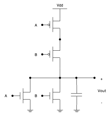
Now, let’s take a look at a pseudo-NMOS implementation of the same NOR gate:
Cell’s implementation goes one step further. The p-type transistor at the top of the circuit and the n-type transistor at the bottom are clocked on non-overlapping phases, meaning that the two clocks aren’t high/low at the same time.
The way in which the gate here works is as follows: inputs are first applied to the logic in between the clock fed transistors. The top transistor’s gate is closed allowing the logic transistors to charge up. The gate is then opened and the lower transistor’s gate is closed to drain the logic transistors to ground. The charge that remains is the output of the circuit.
What’s important about this is that since power is only consumed during two non-overlapping phases, overall power consumption is lower than static CMOS. The downside is that clock signal routing becomes much more difficult.
The other benefit is lower transistor count. In the example of the 2-input NOR gate, our static CMOS design used 4 transistors, while our pseudo-NMOS implementation used 4 transistors as well. But for a 3-input NOR gate, the static CMOS implementation requires 6 transistors, while the pseudo-NMOS implementation requires 5. The reasoning is that for a CMOS circuit, you have 1 p-type transistor for every n-type, while in a pseudo-NMOS circuit you only have two additional transistors beyond the bare minimum required to implement the logic function. For a 100-input NOR gate (unrealistic, but a good example), a static CMOS implementation would require 200 transistors, while a pseudo-NMOS implementation would only require 102.
By making more efficient use of transistors and lowering power consumption, Cell’s pseudo-NMOS logic design enables higher clock frequencies. The added cost is in the manufacturing and design stages:
- As we mentioned before, clock routing becomes increasingly difficult with pseudo-NMOS designs similar to that used in Cell. The clock trees required for Cell are probably fairly complex, but given IBM’s expertise in the field, it’s not an insurmountable problem.
- Designing pseudo-NMOS logic isn’t easy, and there are no widely available libraries from which to pull circuit designs. Once again, given IBM’s size and expertise, this isn’t much of an issue, but it does act as a barrier for entry of smaller chip manufacturers.
- Manufacturing such high speed dynamic logic circuits often requires techniques like SOI, but once again, not a problem for IBM given that they have been working on SOI for quite some time now. There’s no surprise that Cell is manufactured on a 90nm SOI process.


70 Comments
View All Comments
Houdani - Friday, March 18, 2005 - link
I think I missed something fundamental.Can the SPEs be addressed directly by software, or do they have to be fed all of their instructions by the PPE?
If they DO have to be fed be the PPE, I fail to see how the PPE can possibly feed them enough to keep them all working concurrently.
Someone throw me a bone here.
suryad - Friday, March 18, 2005 - link
I thought the G5 was a POWER5 proc. But I could of course be wrong. All I can say is the Cell definitely intriguing as it may be will have a rough road ahead of it and I am quite surprised that these large corporations invested so much in it, cutting edge though it might be. And as for the current forseeable future, I think when multi-core FX processors from AMD comes out, I do not believe there will be anything more devastating than that. Especially once they hit the 3 Ghz barrier with multi-cores enabled and faster DDR2-3 or even RAMBUS memory capabilities.tipoo - Thursday, December 3, 2015 - link
No, G5 was 970 based.Questar - Friday, March 18, 2005 - link
#50,Yes the G5 is a POWER4 derivitive.
Since you were wrong on that, don't think that you know what is significant about the design of POWER5. There were major architechture changes made to the processor.
fitten - Friday, March 18, 2005 - link
The only things new about Cell is its target market and being a single chip. The article mentions the TI DSP chip, but there were other similar architectures as well. One example that I'm familiar with is the MAP1310 board by CSPI. Back then, processes weren't good enough to put all the cores on a single chip but the basic architecture is the same - a PPC core to do the 'normal' stuff and two quad-core DSPs (SHARC) to do the 'work'. This board wasn't successful because it was considered too hard to program to get the performance it promised.... and this opinion is from people who live/breathe real-time systems and multiprocessing codes.The only thing new about Cell is that a) it's all on one chip now and b) the target market is a general marketplace and not a niche.
scrotemaninov - Friday, March 18, 2005 - link
#48. OK, I was under the impression that the G5 was based on the POWER5. You're saying it's based on the POWER4 instead?And the POWER4 and POWER5 aren't really "completely different chips" in the same way that the P4 and P3 are different chips, or in the way that the P4 and the Opteron are different chips. I can give you a list of the differences if you want. Start at http://www.elet.polimi.it/upload/sami/architetture...
The POWER5 is designed to not only be completely compatible with the POWER4 but to also to support all the optimisations from the POWER4. The only things of significance they've done is a) move the L3 cache controller on chip; b) change the various branch predictors to bimodal instead of 1-bit; c) increase the associativity and size of the caches.
Anyway, this is going off topic now...
Jacmert - Friday, March 18, 2005 - link
Rofl. Computer engineering and VLSI design. Gotta love those NMOS/PMOS transistor circuits.I never thought that I'd see stuff from my textbook explained on anandtech.com
saratoga - Friday, March 18, 2005 - link
"#38. You're right that the G5 is a derivative of the POWER5. The POWER5 is dual core, each core with 2way SMT giving a total of 4 'visible' cpus to the OS. The G5 is simply a single core version of the same thing."Err no its not. POWER4 != POWER5. Hence the different names ;)
They're completely different chips.
"Well scrotemaninov I am not disputing that the POWER architecture by IBM is brilliantly done. IBM is definitely one of those companies churning out brilliant and elegant technology always in the background.
But my problem with the POWER technology is from what I understand very limitedly, is that the POWER processors in the Mac machines are a derivative of that architecture right? Why the heck are they so damn slow then?
I mean you can buy an AMD FX 55 based on the crappy legacy x86 arch and it smokes the dual 2.5 GHz Macs easily!! Is it cause of the OS? Because so far from what I have seen, if the Macs are any indication of the performance capabilities of the POWER architecture, the Cell will not be a big hit.
I did read though at www.aceshardware.com benchmark reviews of the POWER5 architecture with some insane number of cores if I recall correctly and the benchmarks were of the charts. They are definitely not what the Macs have installed in them..."
There are slow memeory systems and then theres the one used on the G5. I've heard that you can put 8 Opterons together and still get average access times across all 8 cores that are better then a single G5. Thats probably a good part of the reason the G5 was so much slower then many people thought it would be. The rest is mainly IBM's trouble making them, and their inability to ramp clock speed like they planned on.
scrotemaninov - Friday, March 18, 2005 - link
#38. You're right that the G5 is a derivative of the POWER5. The POWER5 is dual core, each core with 2way SMT giving a total of 4 'visible' cpus to the OS. The G5 is simply a single core version of the same thing.As for the performance, Opteron is pretty much unbeatable for integer-bound applications. Itanium2 is unbeatable for FP applications. POWER5 is somewhere in the middle.
Most desktop applications are going to be integer bound. So it's not at all surprising that you find the G5 'slow' in that respect in comparison to the FX55. Plus, and this is the whole problem with the CELL, there's no point putting dual CPUs in there unless you can utilise them properly. If you have one process going flat out trying to run a heavy application and it's single threaded then you're only using about 1/4 of the CPUs you've bought for that application (for a dual G5 2.5), whereas the Opterons and FX55 stuff is more designed around quick, single threaded applications.
dmens - Friday, March 18, 2005 - link
psuedo-pmos wtf? That's domino logic, it's been around forever, and it's definitely not efficient in terms of power. Oh, and it takes forever to verify timing.