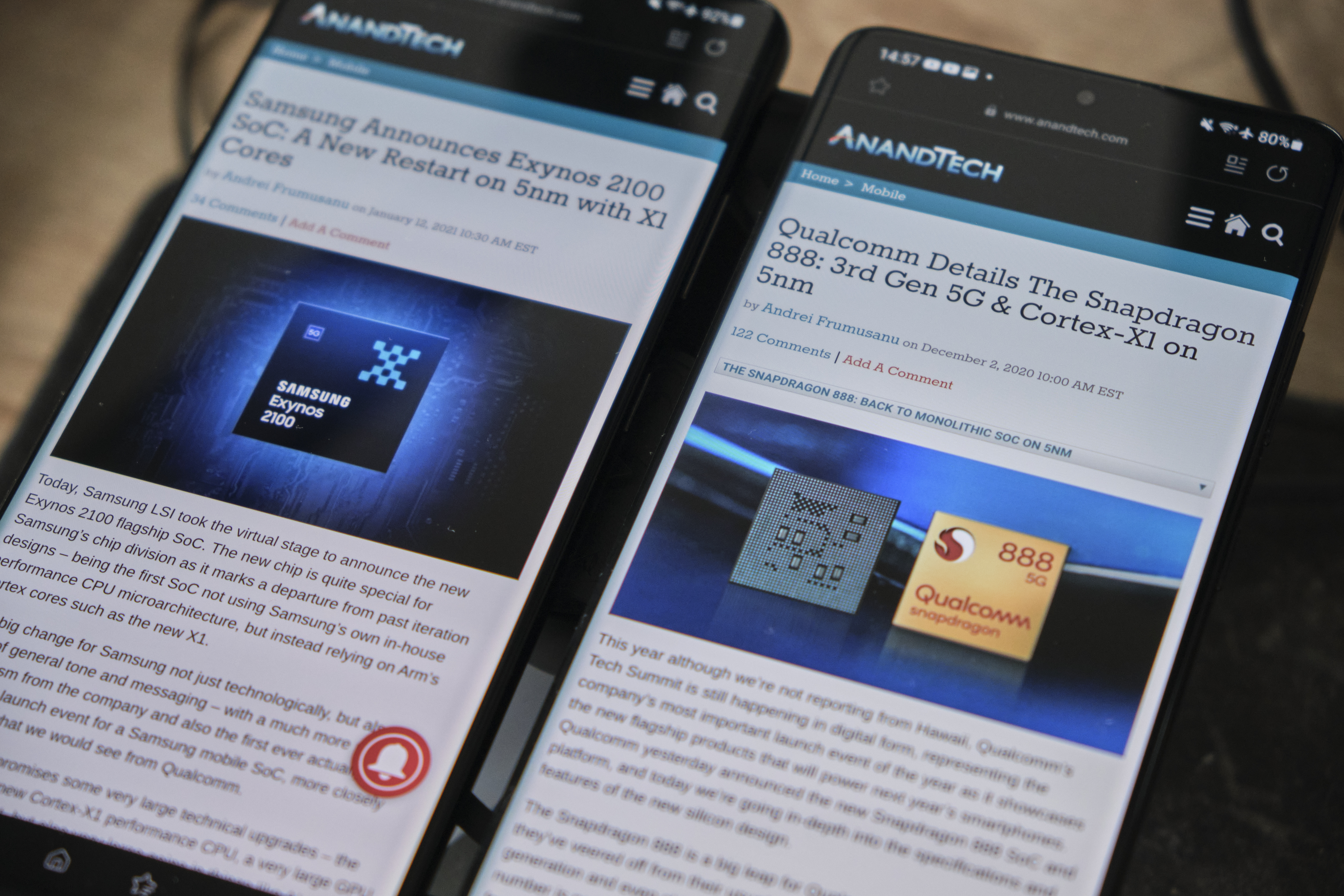
The Snapdragon 888 vs The Exynos 2100: Cortex-X1 & 5nm - Who Does It Better?
by Andrei Frumusanu on February 8, 2021 3:00 AM EST- Posted in
- Mobile
- Samsung
- Qualcomm
- Smartphones
- SoCs
- Snapdragon 888
- Exynos 2100
Conclusion & End Remarks
It’s been a tumultuous and busy week as we’ve only had the new Galaxy S21 Ultra in Snapdragon and Exynos variants for just a few days now, but that’s sufficient as we can generally come to a representative conclusion as to how Qualcomm’s and Samsung’s new generation flagship SoCs will play out in 2021 – and for the most part, it’s probably not what people were expecting.
Starting off with the most hyped up part of the new SoCs (mea culpa), both SoCs are the first to employ Arm’s newest Cortex-X1 cores, the first CPU generation in which Arm really went for a more “performance first” design philosophy. In general, the new CPU IP does live up to its claims, however Arm’s and our own performance projections weren’t met by the new SoCs, as they didn’t quite reach the configurations and clock frequencies we had hoped for 2021 designs. Both Qualcomm and Samsung didn’t invest on an 8MB L3 cache, and in particular Samsung didn’t even don their X1 core with a full 1MB of L2 cache. This does seem to be noticeable in the performance as the Snapdragon 888 does have small performance edge over the Exynos 2100. Samsung’s choice here given their years of wasting lots of silicon on humongous custom CPUs seems to be rather puzzling, but generally both vendors aren’t as aggressive as Apple is on investing die area into caches.
Qualcomm still has a clear memory subsystem advantage as the company has made large strides in latency this generation, and this results in even more extra performance. The Exynos this year surprised us with a much larger system level cache – which however seems to also add to latency and reduce performance.
More worrisome for the Exynos is its weird clock behaviour, with the new chip really struggling in maintaining its peak frequencies other than for very brief moments – the Snapdragon 888’s X1 core had no such issues. My Exynos S21 Ultra chip bin was quite terrible here, but the better silicon on my second S21 doesn’t improve things too much either.
The Exynos 2100’s Cortex-A78 cores are clocked higher than the Snapdragon 888’s, and this show up in performance, however in every-day workloads the DVFS of the Exynos actually behaves more similarly to the Snapdragon as it generally scales things to 2600MHz and only uses the 2808MHz peak frequencies of these cores in brief multi-threaded workloads, as long as thermals even allow it, as even these middle cores can get quite power hungry this generation.
Although both are using the same IP on the same process node, the Exynos 2100’s CPU just look to be more power hungry than the Snapdragon 888’s implementations. Given the apples-to-apples comparison, the only remaining possibility is just a weaker physical design implementation on Samsung LSI’s part – which is actually a point of concern, as we had hoped Exynos SoCs would catch up this year following their ditching of their custom CPU cores. Make no mistake – the new X1 cores are massively improved in performance and efficiency over last year’s M5 cores, it’s just that Qualcomm shows that it can be done even better.
On the GPU side of things, this generation feels wrong to me, and that’s solely due to the peak power levels these new SoCs reach, and which vendors actually left enabled in commercial devices.
Qualcomm had advertised 35% improved GPU performance this generation with the Snapdragon 888, and that might indeed be valid for peak performance, but certainly for Samsung devices that figure is absolutely unreachable for any reasonable amount of gaming periods, as the power consumption is through the roof at over 8W. I don’t see how other vendors might be able to design phones with thermal dissipations that allows for such power levels to actually be maintained without the phone’s skin temperatures exceeding +50°C (122°F), it’s just utterly pointless in my opinion.
In terms of sustained performance, the Snapdragon 888 is generally a 10-15% improvement over the Snapdragon 865 and 865+ - at least in these Samsung devices whose thermal limits and thermal envelopes are similar this generation, attempting to target 42°C peak skin temperatures, although the phones failed to stay below that threshold during the initial few minutes of the performance burn.
On the Exynos 2100 side, Samsung’s +40% performance claim can be considered accurate just for the fact that it generally applies to both peak and sustained performance figures. At peak performance, the SoC is just as absurd at 8W load, which is impossible to maintain. The good news here though, is that when throttling down, the Exynos 2100 is notably better than the Exynos 990 – however that’s not sufficient to catch up to last year’s Snapdragon 865, much less the new Snapdragon 888.
Samsung’s 5LPE process appears to be lacking
We don’t have deeper technical insights as to how Samsung’s process node compares in relation to TSMC’s nodes other than the actual performance of the chips we have in ours hands, so I’m basing my arguments based on the measured data that I’m seeing here.
At lower performance levels, we noted that the 5LPE node doesn’t look to be any different than TSMC’s N7P node, as the A55 cores in the Snapdragon 888 performed and used up exactly the same amount of power as in the Snapdragon 865. At higher performance levels however, we’re seeing regressions – the middle Cortex-A78 cores of the S888 should have been equal power, or at least similar, to the identically clocked A77 cores of the S865, however we’re seeing a 25% power increase this generation.
Similarly, in theory, the Exynos 2100 Cortex-A78 cores at 2.81GHz should have been somewhat similar in power to the 2.84GHz A77 cores of a Snapdragon 865, but it’s again at a 20-25% disadvantage in efficiency.
In fact, both SoCs on the CPU side don’t seem to be able to reach the Kirin 9000’s lower power levels and efficiency even though that chip is running at 3.1GHz – it’s clear to me that TSMC’s N5 node is quite superior in terms of power efficiency.
There are two conclusions here: For Samsung’s Exynos 2100 – it doesn’t really change the situation all that much. 5LPE does seem to be better than 7LPP, and the new chip is definitely more energy efficient than the Exynos 990 – although it does look that the new much more aggressive behaviour of the CPUs, while benefiting performance, can have an impact on battery life. We need more time with the phones to get to a definitive conclusion in that regard.
For Qualcomm’s Snapdragon 888, the new chip’s manufacturing seems to be giving it headwinds. At best, we’re seeing flat energy efficiency, and at worst, we’re seeing generational regressions. This all depends on the operating point, but generally, the new chip seems to be slightly more power hungry than its predecessor – although again, performance has indeed improved. On the CPU side, the performance boost could be noticeable, but more problematic is the sustained GPU performance increase, which is still quite minor. It’s at this point where we have to talk about things other than CPU and GPU, such as Qualcomm’s new Hexagon accelerator, or new camera and ISP capabilities. We weren’t able to test the AI/NPUs today as the software frameworks on the S21 Ultra aren’t complete so it’s something we’ll have to revisit in the future. Looking at all these results, it suddenly makes sense as to why Qualcomm launched another bin/refresh of the Snapdragon 865 in the form of the Snapdragon 870.
Overall, this generation seems a bit lacklustre. Samsung LSI still has work ahead of them in improving fundamental aspects of the Exynos SoCs, maturing the CPU cluster integration with the memory subsystem and adopting AMD’s RDNA architecture GPU in the next generation seem two top items on the to-do list for the next generation, along with just general power efficiency improvements. Qualcomm, while seemingly having executed things quite well this generation, seem to be limited by the process node. We can’t really blame them for this if they couldn’t get the required TSMC volume, but it also means we’re nowhere near in closing the gap with Apple’s SoCs.
In general, I’m sure this year’s devices will be good – but one should have tempered expectations. We'll be following up with full device reviews of the Galaxy S21 Ultras as well as the smaller Galaxy S21 soon - so stay tuned.


123 Comments
View All Comments
Archer_Legend - Tuesday, February 9, 2021 - link
Actually samsung has still M6 cores in its belly, the development team was shut down only after they completed the M6 cores.Difficoult to say if they would have been better than an X1.
However it seems that arm has rushed this whole a78 and X1 thing and samsung rushed to put too much stuff in the cpu with evidently not enough time to do it well
watzupken - Monday, February 8, 2021 - link
Feels like a 20nm all over again. The move to Samsung's fab certainly did not help with the new SD 888 and Samsung's Exynos is able to close the performance gap since they are on the same node. In fact, this review also somewhat confirmed that Nvidia's jump to Samsung's 8nm certainly contributed to the high power consumption and lower clockspeed.s.yu - Monday, February 8, 2021 - link
That would be saying Samsung's 8nm is worse than TSMC 12nm, it's not that bad, it should be a bit better than TSMC 10nm.Spunjji - Monday, February 8, 2021 - link
I assumed they meant higher power relative to TSMC 7nm - of course overall power is still a little higher than Turing on TSMC 12nm because of the higher logic density.Otritus - Monday, February 8, 2021 - link
Samsung's 8nm is based on their 10nm, and can be considered a more refined variant with about a 10% improvement in efficiency. TSMC's 12nm is based on their 16 nm, with about the same efficiency improvements. 10lpp vs 14lpp is about 40% less power. 14lpp was computed to be about 25% less efficient than 16ff+. Which would mean 8lpp has around 20% lower power consumption than 16ff+. Tsmc 10nm should be around 40% less power than 16ff+, so Samsung 8nm is in fact worse than Tsmc 10nm.Silver5urfer - Monday, February 8, 2021 - link
Samsung 8nm for Nvidia doesn't have much impact in the Desktop PEG scene. Because the GPUs are already heavy on power consumption. Having a TSMC will make it efficient but it won't help with temps / clocks or the performance, always a new node helps with either get perf boost or efficiency.Nvidia wanted cheap manufacturing for it's GPUs and more volume. But the latter is busted due to artificially pumping up this BS by Mining craze & corona problem. That's why A100 is on TSMC 7N instead of Samsung, because HPC and other hyperscalers need efficiency.
In mobile it matters a lot due to the stupid Li Ion garbage tech.
Otritus - Monday, February 8, 2021 - link
Efficiency for desktop gpus matters a lot. At best you are limited by temperature and noise, at worst you are also limited by power consumption (primarily oem pcs). If a cooler can dissipate 375 watts at an acceptable noise and temperature threshold, then that's the max power the gpu can ship at(the ceiling is lower if overclocking headroom is considered).Switching to tsmc will help temperatures, performance, and clock. Lower power consumption means lower temperatures. The tsmc node can also clock higher which drives performance up. If using tsmc allows the chip to clock n% higher at the same power, ship it with n/2% more frequency, and now performance and oc headroom is higher, and temps and power draw are lower.
Spunjji - Thursday, February 11, 2021 - link
Both of the major manufacturer's top-end GPUs are limited by power input and heat dissipation - that's why they rarely perform much better than the next tier down, despite having significantly more execution resources. They do better on a performance-per-watt basis, though, because they're operating at a more sane part of the efficiency curve.geoxile - Monday, February 8, 2021 - link
Tsmc 12/16nm was roughly on par with Samsung 14nm.melgross - Monday, February 8, 2021 - link
Yes, when Apple split its SoC production between Samsung and TSMC that one year when they were looking to replace Samsung with TSMC, it was found here, and in other places, that TSMC’ s larger process was 20% more power efficient than Samsung’s smaller process. I think it was the 14 node for Samsung and the 16 for TSMC.So nothing seems to have changed. Samsung’s process technology remains inferior to that of TSMC.