The Snapdragon 888 vs The Exynos 2100: Cortex-X1 & 5nm - Who Does It Better?
by Andrei Frumusanu on February 8, 2021 3:00 AM EST- Posted in
- Mobile
- Samsung
- Qualcomm
- Smartphones
- SoCs
- Snapdragon 888
- Exynos 2100
Memory Subsystem & Latency: Quite Different
The memory subsystem comparisons for the Snapdragon 888 and Exynos 2100 are very interesting for a few couple of reasons. First of all – these new SoCs are the first to use new higher-frequency LPDDR5-6400 memory, which is 16% faster than that of last year’s LPDRR5-5500 DRAM used in flagship devices.
On the Snapdragon 888 side of things, Qualcomm this generation has said that they have made significant progress in improving memory latency – a point of contention that’s generally been a weak point of the previous few generations, although they always did keep improving things gen-on-gen.
On the Exynos 2100 side, Samsung’s abandonment of their custom cores also means that the SoC is now very different to the Exynos 990. The M5 used to have a fast-path connection between the cores and the memory controllers – exactly how Samsung reimplemented this in the Exynos 2100 will be interesting.
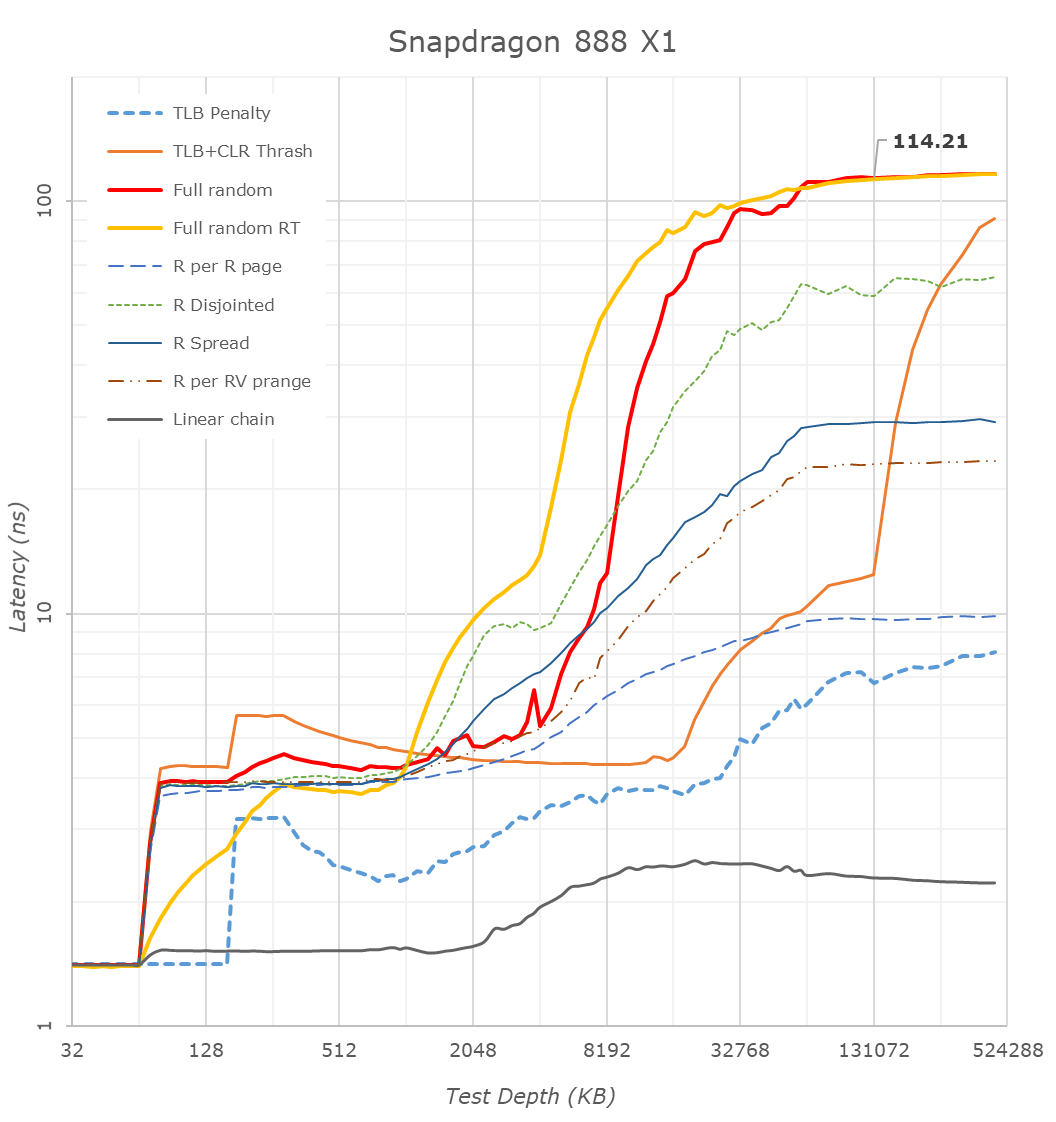
Starting things off with the new Snapdragon 888, we are seeing some very significant changes compared to the Snapdragon 865 last year. Full random memory latency went down from 138ns to 114ns, which is a massive generation gain given that Arm always quotes that 4ns of latency equals 1% of performance.
Samsung’s Exynos 2100 on the other hand doesn’t look as good: At around 136ns at 128MB test depth, this is quite worse than the Snapdragon 888, and actually a regression compared to the Exynos 990 at 131ns.
Looking closer at the cache hierarchies, we’re seeing 64KB of L1 caches for both X1 designs – as expected.
What’s really weird though is the memory patterns of the X1 and A78 cores as they transition from the L2 caches to the L3 caches. Usually, you’d expect a larger latency hump into the 10’s of nanoseconds, however on both the Cortex-X1 and Cortex-A78 on both the Snapdragon and Exynos we’re seeing L3 latencies between 4-6ns which is far faster than any previous generation L3 and DSU design we’ve seen from Arm.
After experimenting a bit with my patterns, the answer to this weird behaviour is quite amazing: Arm is prefetching all these patterns, including the “full random” memory access pattern. My tests here consist of pointer-chasing loops across a given depth of memory, with the pointer-loop being closed and always repeated. Arm seems to have a new temporal prefetcher that recognizes arbitrary memory patterns and will latch onto them and prefetch them in further iterations.
I re-added an alternative full random access pattern test (“Full random RT”) into the graph as alternative data-points. This variant instead of being pointer-chase based, will compute a random target address at runtime before accessing it, meaning it’ll be always a different access pattern on repeated loops of a given memory depth. The curves here aren’t as nice and they aren’t as tight as the pointer-chase variant because it currently doesn’t guarantee that it’ll visit every cache line at a given depth and it also doesn’t guarantee not revisiting a cache line within a test depth loop, which is why some of the latencies are lower than that of the “Full random” pattern – just ignore these parts.
This alternative patterns also more clearly reveals the 512KB versus 1MB L2 cache differences between the Exynos’ X1 core and the Snapdragon X1 core. Both chips have 4MB of L3, which is pretty straightforward to identify.
What’s odd about the Exynos is the linear access latencies. Unlike the Snapdragon whose latency grows at 4MB and remains relatively the same, the Exynos sees a second latency hump around the 10MB depth mark. It’s hard to see here in the other patterns, but it’s also actually present there.
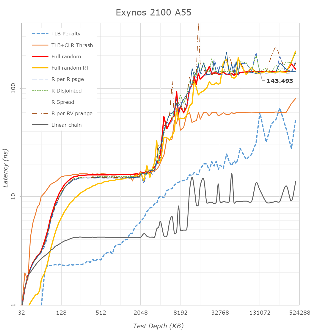
This post-4MB L3 cache hierarchy is actually easier to identify from the perspective of the Cortex-A55 cores. We see a very different pattern between the Exynos 2100 and the Snapdragon 888 here, and again confirms that there’s lowered latencies up until around 10MB depth.
During the announcement of the Exynos 2100, Samsung had mentioned they had improved and included “better cache memory”, which in context of these results seems to be pointing out that they’ve now increased their system level cache from 2MB to 6MB. I’m not 100% sure if it’s 6 or 8MB, but 6 seems to be a safe bet for now.
In these A55 graphs, we also see that Samsung continues to use 64KB L2 caches, while Qualcomm makes use of 128KB implementations. Furthermore, it looks like the Exynos 2100 makes available to the A55 cores the full speed of the memory controllers, while the Snapdragon 888 puts a hard limit on them, and hence the very bad memory latency, similarly to how Apple does the same in their SoCs when just the small cores are active.
Qualcomm seems to have completely removed access of the CPU cluster to the SoC’s system cache, as even the Cortex-A55 cores don’t look to have access to it. This might explain why the CPU memory latency this generation has been greatly improved – as after all, memory traffic had to do one whole hop less this generation. This also in theory would put less pressure on the SLC, and allow the GPU and other blocks to more effectively use its 3MB size.


123 Comments
View All Comments
Archer_Legend - Tuesday, February 9, 2021 - link
Actually samsung has still M6 cores in its belly, the development team was shut down only after they completed the M6 cores.Difficoult to say if they would have been better than an X1.
However it seems that arm has rushed this whole a78 and X1 thing and samsung rushed to put too much stuff in the cpu with evidently not enough time to do it well
watzupken - Monday, February 8, 2021 - link
Feels like a 20nm all over again. The move to Samsung's fab certainly did not help with the new SD 888 and Samsung's Exynos is able to close the performance gap since they are on the same node. In fact, this review also somewhat confirmed that Nvidia's jump to Samsung's 8nm certainly contributed to the high power consumption and lower clockspeed.s.yu - Monday, February 8, 2021 - link
That would be saying Samsung's 8nm is worse than TSMC 12nm, it's not that bad, it should be a bit better than TSMC 10nm.Spunjji - Monday, February 8, 2021 - link
I assumed they meant higher power relative to TSMC 7nm - of course overall power is still a little higher than Turing on TSMC 12nm because of the higher logic density.Otritus - Monday, February 8, 2021 - link
Samsung's 8nm is based on their 10nm, and can be considered a more refined variant with about a 10% improvement in efficiency. TSMC's 12nm is based on their 16 nm, with about the same efficiency improvements. 10lpp vs 14lpp is about 40% less power. 14lpp was computed to be about 25% less efficient than 16ff+. Which would mean 8lpp has around 20% lower power consumption than 16ff+. Tsmc 10nm should be around 40% less power than 16ff+, so Samsung 8nm is in fact worse than Tsmc 10nm.Silver5urfer - Monday, February 8, 2021 - link
Samsung 8nm for Nvidia doesn't have much impact in the Desktop PEG scene. Because the GPUs are already heavy on power consumption. Having a TSMC will make it efficient but it won't help with temps / clocks or the performance, always a new node helps with either get perf boost or efficiency.Nvidia wanted cheap manufacturing for it's GPUs and more volume. But the latter is busted due to artificially pumping up this BS by Mining craze & corona problem. That's why A100 is on TSMC 7N instead of Samsung, because HPC and other hyperscalers need efficiency.
In mobile it matters a lot due to the stupid Li Ion garbage tech.
Otritus - Monday, February 8, 2021 - link
Efficiency for desktop gpus matters a lot. At best you are limited by temperature and noise, at worst you are also limited by power consumption (primarily oem pcs). If a cooler can dissipate 375 watts at an acceptable noise and temperature threshold, then that's the max power the gpu can ship at(the ceiling is lower if overclocking headroom is considered).Switching to tsmc will help temperatures, performance, and clock. Lower power consumption means lower temperatures. The tsmc node can also clock higher which drives performance up. If using tsmc allows the chip to clock n% higher at the same power, ship it with n/2% more frequency, and now performance and oc headroom is higher, and temps and power draw are lower.
Spunjji - Thursday, February 11, 2021 - link
Both of the major manufacturer's top-end GPUs are limited by power input and heat dissipation - that's why they rarely perform much better than the next tier down, despite having significantly more execution resources. They do better on a performance-per-watt basis, though, because they're operating at a more sane part of the efficiency curve.geoxile - Monday, February 8, 2021 - link
Tsmc 12/16nm was roughly on par with Samsung 14nm.melgross - Monday, February 8, 2021 - link
Yes, when Apple split its SoC production between Samsung and TSMC that one year when they were looking to replace Samsung with TSMC, it was found here, and in other places, that TSMC’ s larger process was 20% more power efficient than Samsung’s smaller process. I think it was the 14 node for Samsung and the 16 for TSMC.So nothing seems to have changed. Samsung’s process technology remains inferior to that of TSMC.