The Snapdragon 888 vs The Exynos 2100: Cortex-X1 & 5nm - Who Does It Better?
by Andrei Frumusanu on February 8, 2021 3:00 AM EST- Posted in
- Mobile
- Samsung
- Qualcomm
- Smartphones
- SoCs
- Snapdragon 888
- Exynos 2100
5nm / 5LPE: What do we know?
Starting off with the biggest new change of this generation, both the Snapdragon 888 and the Exynos 2100 are manufactured on Samsung’s new 5nm process node, which is the biggest unknown in today’s comparison.
What’s important to remember is that although Samsung calls this node 5nm, its design and characteristics are more similar to that of their 7nm node. Key new characteristics of the new node here are the reintroduction of single diffusion breaks (SDB) on an EUV process node, as well as slight changes in the cell libraries of the process.
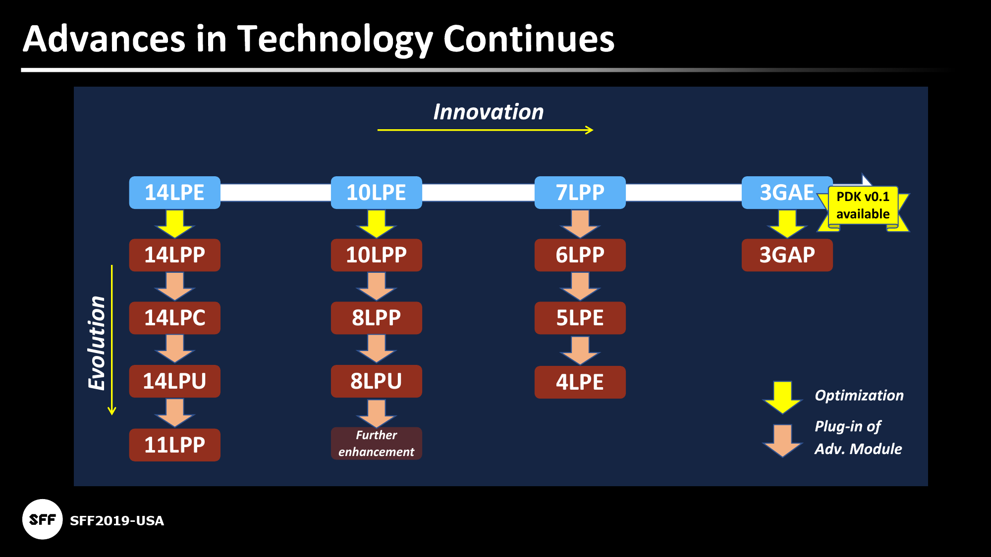
| Advertised PPA Improvements of New Process Technologies Data announced by companies during conference calls, press briefings and in press releases |
||||||
| 7LPP vs 10LPE |
6LPP vs 7LPP |
5LPE vs 7LPP |
3GAE vs 7LPP |
|||
| Power | 50% | lower | 20% | 50% | ||
| Performance | 20% | ? | 10% | 35% | ||
| Area Reduction | 40% | ~9% | <20% | 40% | ||
Per Samsung’s own numbers, the foundry claims that 5LPE is either 20% lower power than 7LPP, or 10% more performance. These are actually quite important figures to put into context, particularly when we’re comparing designs which are manufactured on TSMC’s process nodes.
In least year’s review of the Galaxy S20 series and the Exynos 990 and Snapdragon 865 SoCs, an important data-point that put things into context was Qualcomm’s Snapdragon 765 SoC which was also manufactured on Samsung’s 7LPP node, and featuring Cortex-A76 cores. In that comparison we saw that The Exynos 990 and the Snapdragon 765’s A76 cores behaves very similarly in terms of power consumption, however they fell behind TSMC-based Cortex-A76 cores by anywhere from 20% to 30%.
In that context, Samsung’s 5LPE process node improving power by 20% would mean they’d only be catching up with TSMC’s 7nm nodes.
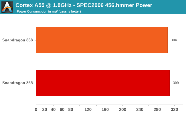
An interesting comparison to make – and probably one of the rare ones we’re actually able to achieve today, is the comparison between the Cortex-A55 cores inside of both the Snapdragon 865 and the new Snapdragon 888. Both SoCs feature the same IP cores, clock them at the same 1.8GHz frequency, and both feature the same amount of L2 cache, with their only real difference being their process nodes.
Using SPEC’s 456.hmmer – because it’s a workload that primarily resides in the lower cache hierarchies and thus, we avoid any impact of the possibly different memory subsystem, we can see that both SoCs’ power consumption indeed is almost identical, with performance also being identical with a score of 6.84 versus 6.81 in favour of the new Snapdragon 888.
So at least at first glance, our theory that Samsung’s 5LPE merely just catches up with the power consumption and power efficiency of TSMC’s N7/N7P nodes seems to be valid – at least at these frequencies.

Further interesting data is the voltage curves of the CPUs on the Exynos 2100. I’ve extracted the frequency voltages tables of both my devices, a regular S21 and an S21 Ultra, with the above curves being the better binned chip inside of the smaller S21.
Generationally, Samsung seems to have been able to greatly reduce voltages this generation. On the Cortex-A55 cores, the cores now only require 800mV at 2GHz whilst the Exynos 990 last year in our review unit they required over 1050mV. Similarly, although the comparison isn’t apples-to-apples, the Cortex-A78 cores at 2.5GHz only require 862mV, while the Cortex-A76 cores of the previous generation required also 1050mV.
What’s also very interesting to see is the voltage curves of the Cortex-X1 cores versus the Cortex-A78 cores: they’re both nigh identical to each other, which actually lines up with Arm’s claims that the new X1 cores have the same frequency capabilities as the A78 cores, only being larger and increasing their power consumption linearly in relation to their frequency.
Samsung’s frequency tables indicate that they had been testing the A55 up to 2.6GHz, and the X1 and A78 cores up to 3.2GHz – however voltages here are quite higher and it’s also likely SLSI wouldn’t have been able to achieve similar chip yields.
Unfortunately, I wasn’t able to extract data from my Snapdragon 888 S21 Ultra, so I can’t tell exactly where it falls in terms of voltages compared to the Exynos 2100. One thing I can confirm as being quite different between the two SoCs is that Samsung does actually give the Exynos 2100’s Cortex-X1 core its own dedicated voltage rail and PMIC regulator, while the Snapdragon 888 shares the same voltage rail across the X1 and A78 cores. In theory, that could mean that in more mixed-thread workloads, the Exynos has the opportunity to be more power efficiency than the Snapdragon 888.
Generally, the one thing I want people to take away here is that although Samsung calls this their 5nm node, it’s quite certain that it will not perform the same as TSMC’s 5nm node. Usually we don’t care about density all too much, however performance and power efficiency are critical aspects that effect the silicon and the end-products’ experiences.


123 Comments
View All Comments
Andrei Frumusanu - Tuesday, February 9, 2021 - link
I don't have 5G coverage here so it's not feasible for me to test.Edwardmcardle - Wednesday, February 10, 2021 - link
Will you be testing reception differences e.g. 4g and wifi? Fantastic write up as always!Dorkaman - Tuesday, February 9, 2021 - link
Different s21 ultra phones can have different performance says tech chaphttps://youtu.be/yuNNmf2gIRc
I guess this is due to binning and his tests show his Exonys 2100 is in the middle. Strange. Also, the battery life is better on the 888 and external temps are about the samd.
serendip - Tuesday, February 9, 2021 - link
All this really doesn't look good for Windows on ARM if we're stuck with hot and hungry Qualcomm chips on Samsung 5nm. The 8cx and SQ on TSMC 7nm were very efficient but that's with slower A76 cores. I'm hoping a quad-X1 design on TSMC 5nm will be in the next iteration of the Surface Pro X or Galaxy Book S.Raqia - Tuesday, February 9, 2021 - link
Disappointing sustained performance, however the S21 series lacks the phase change vapor chamber cooling solution of the S20's:https://9to5google.com/2021/01/18/samsung-galaxy-s...
vs
https://www.ifixit.com/News/43501/why-samsung-buil...
Notably the Mi11 has this:
https://gadgettendency.com/a-triple-chamber-as-a-s...
This makes for better subsequent runs but the SoCs built on 5LPE are still disappointing.
iphonebestgamephone - Wednesday, February 10, 2021 - link
Mi 11 may have the vapor chamber for better cooling, but it also allows for a higher battery temperature. If they throttled at the same temps we could see how useful that thing actually is.dudedud - Wednesday, February 10, 2021 - link
Not all S20s had that vapor chamber. Some just had a graphene layer, which in theory would give similar results. Don't know if the S21 uses graphene tho.darkich - Wednesday, February 10, 2021 - link
The battery life benchmarks are indication of how actually invalid the whole Anantech's premise is.Pretty much ALL actual real usage tests have shown BIG improvements in the autonomy between the S20/S21 yet Andrei wants us to believe in the stupid benchmark test that shows "regression" between Exynos 990 and Exynos 2100.
What a joke..
ChrisGX - Sunday, February 14, 2021 - link
I would say these results are incomplete rather than invalid. The PCMark Work 2.0 - Battery Life test is a demanding mixed usage benchmark. When running that benchmark it isn't exactly a shock that the Exynos 2100 S21 Ultra should return very slightly reduced battery life than the Exynos 990 S20 Ultra. Anandtech isn't alone in noting that when processing demanding workloads the Exynos 2100 draws more power (on average) than the Exynos 990. Andrei, for his part, is explicit that the Exynos 2100 is also significantly more performant than its predecessor. He does say that the increased performance wasn’t just achieved through improved efficiency, but also through greater power usage and it is hard to dispute that looking at the numbers.There is a gap in the data however. The full PCMark Work 2.0 - Battery Life test involves a Work performance score that gives a more complete picture of how much work/the rate that work is being completed while executing the test. That would be very useful information to have. Still, it is undoubtedly the case that the reduction in battery life that Andrei mentions is not due to a regression but rather the increased rate that the Exynos 2100 is executing work (when processing demanding mixed usage workloads). While that information isn't provided in connection to the PCMark Work 2.0 - Battery Life test the GFXBench GPU heavy test data (arranged in Power Efficiency tables) does confirm the high power draw of the Exynos 2100 during peak performance bursts (which must bump up average power consumption as well) even as that chip roundly outperforms the Exynos 990.
Indeed, heavy mixed usage workloads are not going to put the Exynos 2100 battery life in the best light. Still, Andrei did show the results from a Web Browsing Battery Life test that undoubedly will be useful to a lot of phone users who don't view the results of the PCMark Work 2.0 - Battery Life test as having a lot of relevance for them. But, I, for one, am happy to have that information.
Andrei seems to be adding to/reworking the battery life data in this review.
https://benchmarks.ul.com/pcmark-android
https://s3.amazonaws.com/download-aws.futuremark.c...
sachouba - Wednesday, February 10, 2021 - link
Nice peak power consumption!It doesn't seem unlikely that we'll end up with a situation similar to Apple's battery gate on Snapdragon 888 devices, in a few years. Way to go!