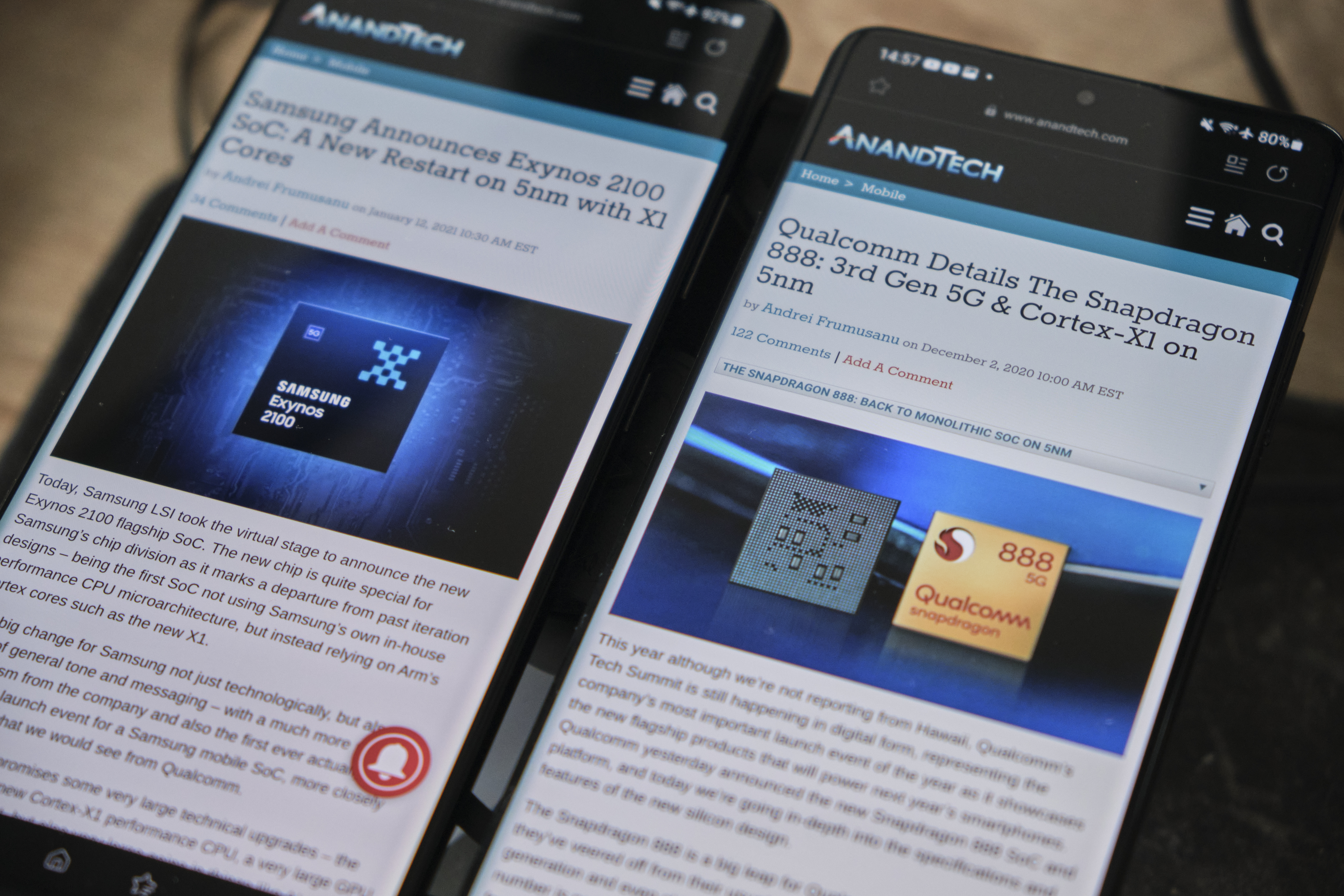
The Snapdragon 888 vs The Exynos 2100: Cortex-X1 & 5nm - Who Does It Better?
by Andrei Frumusanu on February 8, 2021 3:00 AM EST- Posted in
- Mobile
- Samsung
- Qualcomm
- Smartphones
- SoCs
- Snapdragon 888
- Exynos 2100
Conclusion & End Remarks
It’s been a tumultuous and busy week as we’ve only had the new Galaxy S21 Ultra in Snapdragon and Exynos variants for just a few days now, but that’s sufficient as we can generally come to a representative conclusion as to how Qualcomm’s and Samsung’s new generation flagship SoCs will play out in 2021 – and for the most part, it’s probably not what people were expecting.
Starting off with the most hyped up part of the new SoCs (mea culpa), both SoCs are the first to employ Arm’s newest Cortex-X1 cores, the first CPU generation in which Arm really went for a more “performance first” design philosophy. In general, the new CPU IP does live up to its claims, however Arm’s and our own performance projections weren’t met by the new SoCs, as they didn’t quite reach the configurations and clock frequencies we had hoped for 2021 designs. Both Qualcomm and Samsung didn’t invest on an 8MB L3 cache, and in particular Samsung didn’t even don their X1 core with a full 1MB of L2 cache. This does seem to be noticeable in the performance as the Snapdragon 888 does have small performance edge over the Exynos 2100. Samsung’s choice here given their years of wasting lots of silicon on humongous custom CPUs seems to be rather puzzling, but generally both vendors aren’t as aggressive as Apple is on investing die area into caches.
Qualcomm still has a clear memory subsystem advantage as the company has made large strides in latency this generation, and this results in even more extra performance. The Exynos this year surprised us with a much larger system level cache – which however seems to also add to latency and reduce performance.
More worrisome for the Exynos is its weird clock behaviour, with the new chip really struggling in maintaining its peak frequencies other than for very brief moments – the Snapdragon 888’s X1 core had no such issues. My Exynos S21 Ultra chip bin was quite terrible here, but the better silicon on my second S21 doesn’t improve things too much either.
The Exynos 2100’s Cortex-A78 cores are clocked higher than the Snapdragon 888’s, and this show up in performance, however in every-day workloads the DVFS of the Exynos actually behaves more similarly to the Snapdragon as it generally scales things to 2600MHz and only uses the 2808MHz peak frequencies of these cores in brief multi-threaded workloads, as long as thermals even allow it, as even these middle cores can get quite power hungry this generation.
Although both are using the same IP on the same process node, the Exynos 2100’s CPU just look to be more power hungry than the Snapdragon 888’s implementations. Given the apples-to-apples comparison, the only remaining possibility is just a weaker physical design implementation on Samsung LSI’s part – which is actually a point of concern, as we had hoped Exynos SoCs would catch up this year following their ditching of their custom CPU cores. Make no mistake – the new X1 cores are massively improved in performance and efficiency over last year’s M5 cores, it’s just that Qualcomm shows that it can be done even better.
On the GPU side of things, this generation feels wrong to me, and that’s solely due to the peak power levels these new SoCs reach, and which vendors actually left enabled in commercial devices.
Qualcomm had advertised 35% improved GPU performance this generation with the Snapdragon 888, and that might indeed be valid for peak performance, but certainly for Samsung devices that figure is absolutely unreachable for any reasonable amount of gaming periods, as the power consumption is through the roof at over 8W. I don’t see how other vendors might be able to design phones with thermal dissipations that allows for such power levels to actually be maintained without the phone’s skin temperatures exceeding +50°C (122°F), it’s just utterly pointless in my opinion.
In terms of sustained performance, the Snapdragon 888 is generally a 10-15% improvement over the Snapdragon 865 and 865+ - at least in these Samsung devices whose thermal limits and thermal envelopes are similar this generation, attempting to target 42°C peak skin temperatures, although the phones failed to stay below that threshold during the initial few minutes of the performance burn.
On the Exynos 2100 side, Samsung’s +40% performance claim can be considered accurate just for the fact that it generally applies to both peak and sustained performance figures. At peak performance, the SoC is just as absurd at 8W load, which is impossible to maintain. The good news here though, is that when throttling down, the Exynos 2100 is notably better than the Exynos 990 – however that’s not sufficient to catch up to last year’s Snapdragon 865, much less the new Snapdragon 888.
Samsung’s 5LPE process appears to be lacking
We don’t have deeper technical insights as to how Samsung’s process node compares in relation to TSMC’s nodes other than the actual performance of the chips we have in ours hands, so I’m basing my arguments based on the measured data that I’m seeing here.
At lower performance levels, we noted that the 5LPE node doesn’t look to be any different than TSMC’s N7P node, as the A55 cores in the Snapdragon 888 performed and used up exactly the same amount of power as in the Snapdragon 865. At higher performance levels however, we’re seeing regressions – the middle Cortex-A78 cores of the S888 should have been equal power, or at least similar, to the identically clocked A77 cores of the S865, however we’re seeing a 25% power increase this generation.
Similarly, in theory, the Exynos 2100 Cortex-A78 cores at 2.81GHz should have been somewhat similar in power to the 2.84GHz A77 cores of a Snapdragon 865, but it’s again at a 20-25% disadvantage in efficiency.
In fact, both SoCs on the CPU side don’t seem to be able to reach the Kirin 9000’s lower power levels and efficiency even though that chip is running at 3.1GHz – it’s clear to me that TSMC’s N5 node is quite superior in terms of power efficiency.
There are two conclusions here: For Samsung’s Exynos 2100 – it doesn’t really change the situation all that much. 5LPE does seem to be better than 7LPP, and the new chip is definitely more energy efficient than the Exynos 990 – although it does look that the new much more aggressive behaviour of the CPUs, while benefiting performance, can have an impact on battery life. We need more time with the phones to get to a definitive conclusion in that regard.
For Qualcomm’s Snapdragon 888, the new chip’s manufacturing seems to be giving it headwinds. At best, we’re seeing flat energy efficiency, and at worst, we’re seeing generational regressions. This all depends on the operating point, but generally, the new chip seems to be slightly more power hungry than its predecessor – although again, performance has indeed improved. On the CPU side, the performance boost could be noticeable, but more problematic is the sustained GPU performance increase, which is still quite minor. It’s at this point where we have to talk about things other than CPU and GPU, such as Qualcomm’s new Hexagon accelerator, or new camera and ISP capabilities. We weren’t able to test the AI/NPUs today as the software frameworks on the S21 Ultra aren’t complete so it’s something we’ll have to revisit in the future. Looking at all these results, it suddenly makes sense as to why Qualcomm launched another bin/refresh of the Snapdragon 865 in the form of the Snapdragon 870.
Overall, this generation seems a bit lacklustre. Samsung LSI still has work ahead of them in improving fundamental aspects of the Exynos SoCs, maturing the CPU cluster integration with the memory subsystem and adopting AMD’s RDNA architecture GPU in the next generation seem two top items on the to-do list for the next generation, along with just general power efficiency improvements. Qualcomm, while seemingly having executed things quite well this generation, seem to be limited by the process node. We can’t really blame them for this if they couldn’t get the required TSMC volume, but it also means we’re nowhere near in closing the gap with Apple’s SoCs.
In general, I’m sure this year’s devices will be good – but one should have tempered expectations. We'll be following up with full device reviews of the Galaxy S21 Ultras as well as the smaller Galaxy S21 soon - so stay tuned.


123 Comments
View All Comments
serendip - Monday, February 8, 2021 - link
I'm interested in what this means for the SD8cx successor. A 30% increase from using one or two X1 cores would be great, I'm using the SQ2 chip and that's fast enough for typical office tasks. That's still not enough to get within striking range of the M1 or even A14. What the heck is in those Firestorms that makes them so fast?On memory subsystems, what are Qualcomm and Samsung doing wrong compared to Apple and HiSilicon? The M1's memory bandwidth is astonishingly high but that's from using custom parts. HiSilicon is doing a great job using standard ARM interconnects.
Agreed on the stupidly high GPU clocking. The SQ2 has a beefy GPU that performs well but it can get hot even in a large tablet form factor. It's time to stop the marketing departments from forcing engineers to chase pointless metrics.
ikjadoon - Monday, February 8, 2021 - link
>What the heck is in those Firestorms that makes them so fast?A trifecta that I share with people because this question comes up so often.
Technical Part 1: https://www.anandtech.com/show/16226/apple-silicon...
Technical Part 2: https://www.anandtech.com/show/16252/mac-mini-appl...
Consumer + Approachable: https://www.youtube.com/watch?v=3SG5e4z-Ygg
Technical Background + More Approachable: https://www.youtube.com/watch?v=cAjarAgf0nI
As Upscaled wrote, "It's not magic. It's good design." And why don't AMD / Intel have these same good designs? The videos above give thorough answers. For example, the last link explains why everyone cares Firestorm (A14) and Lightning (A13) have an 8-wide decode, which is one of many major "better designs" versus competing Arm & x86 CPUs.
ikjadoon - Monday, February 8, 2021 - link
Uh, wait. Delete. I definitely skipped too much of that one. What on Earth is he going on about 1T vs 1C?~~ Consumer + Approachable: https://www.youtube.com/watch?v=3SG5e4z-Ygg ~~
Wow, I'm a little stunned at how bad this Upscaled video is. The Dev Doc + AnandTech are much more reliable.
Nicon0s - Monday, February 8, 2021 - link
LoL, Engadget.He keeps saying multithreading when he means SMT or Hyperthreading(Intel's version of SMT).
ikjadoon - Monday, February 8, 2021 - link
Yes! Never mind 1T / 1C have shown negligence IPC differences in general computing. 1% at best. Please go test an i5-8600K vs an i7-8700K: one has SMT, one does not. Terrible to see the WCCFTech disinformation cycle reach a mainstream audience so quickly.https://www.anandtech.com/show/16261/investigating...
And then he, out of left field, throws up a Cinebench multi-core score: "See? Intel and Apple are actually very close to each other." But, his comparison was the 4+4 M1 vs an 8C Intel...
I wish I could edit comments. I give up on consumer YouTube videos; I saw his earlier interview with RISC's founders and it seemed halfway decent. I'm a fool.
Archer_Legend - Tuesday, February 9, 2021 - link
Don't be offended but I think that what you posted is completely bs.First of all you are comparing arm64 cpus and x86 cpus, second the arm 64 cores used by apple are very arguably faster than the x86 cores of for example a ryzen cpu.
The second thing which I would want to point out is that about the widht of the pipeline, it is not that apple is a genious or intel and amd are stupid: the x86 architecture was built to have a narrowish pipeline and do more cycles in fact the width of the pipeline in intel and amd cpus is as wide as it gets.
Arm arch on the other end lets you use a wider pipeline, however saying using a narrower or wider pipeline is better or not is pointless because performance comes down to how you organise the cpu around that specific pipeline so....
leledumbo - Monday, February 8, 2021 - link
> What the heck is in those Firestorms that makes them so fast?The same thing since A9 again (CMIIW): super wide decoder + super big cache. Apple isn't stingy when it comes to die size and Apple SoCs are always bigger than Snapdragon on the same generation and process node. 4mm^2 difference is huge when we're talking at nm level. What's weird, Exynos is even bigger but can't match these two. No idea what Samsung put there.
Santoval - Tuesday, February 9, 2021 - link
"What's weird, Exynos is even bigger but can't match these two. No idea what Samsung put there."This is probably due to TSMC having a *far* denser 5nm process node compared to Samsung's process 5nm node. Per the article below TSMC's 5nm node tops at 173 million transistors per mm^2 while Samsung's 5nm node reaches only 126.5 MTr/mm^2 (i.e. barely denser than TSMC's second gen 7nm+ node) due to much more, er, "conservative" design choices (Samsung basically just switched from DDB cells in 7nm to SDB cells; the article explains what that means).
What is often not clear is that the quoted transistor densities of each process node are always the *maximum* transistor densities, not the actual transistor densities used to fab a die. For instance Intel have three different 10nm node variants with three different densities, a low, mid and high density variant (ranging I believe from ~55 million to ~100 million transistors per mm^2). The last one is the only one that has been widely reported, the other two were intended for the tech savvy press and audience.
Each Intel 10nm die has a mix of all three libraries, but each design is (obviously) *fixed* with a precise mix of the three. The desktop parts always have a higher percentage of low density cells because these need to clock higher, and vice versa for the mobile parts. Mobile phones are efficiency focused, so their SoCs have the highest percentage of the highest density variant of each process node that is possible (without hindering performance too much).
That is an additional reason their clocks top at ~3 GHz. Since the two SoCs of the article are both mobile SoCs of an almost identical design we can assume a roughly equivalent percentage of the highest density cells each process node maxes out at. Thus, if all else was being equal (including the same iGPU) Samsung's SoC would have a roughly ~27% larger die than TSMC's SoC. That must be the main reason Samsung kept the cache sizes of the X1 and the A55 cores low.
Santoval - Tuesday, February 9, 2021 - link
p.s. Sorry, I forgot the link to the article :https://semiwiki.com/semiconductor-manufacturers/s...
Santoval - Tuesday, February 9, 2021 - link
p.s.2 I just noticed that the Snapdragon 888 is also fabbed with Samsung's 5nm node. While that rendered the comparison between the two SoCs in my above comment moot the other things I pointed out might have some "academic" value regarding process nodes (I have no away to delete the comment anyway..).