The Snapdragon 888 vs The Exynos 2100: Cortex-X1 & 5nm - Who Does It Better?
by Andrei Frumusanu on February 8, 2021 3:00 AM EST- Posted in
- Mobile
- Samsung
- Qualcomm
- Smartphones
- SoCs
- Snapdragon 888
- Exynos 2100
GPU Performance & Power: Very, Very Hot
Moving onto the GPU side of things, I was very intrigued coming into this comparison, as both Qualcomm as well as Samsung LSI had made promises of enormous performance upgrades in the range of 35% and 40% respectively. We didn’t exactly know how Qualcomm achieved these performance gains given this year’s rather opaquer reveal of the Snapdragon 888. On the Exynos side, I was immediately dubious about Samsung’s 40% claim given that the new Mali-G78 was only meant to be a small generational performance and efficiency boost, as well as the process node having only a 20% power efficiency gain, however the Exynos 990 was in a bad position so maybe it was possible to achieve. Given a lack of large architectural as well as process node improvements, the large performance improvements must thus come from large power increases.
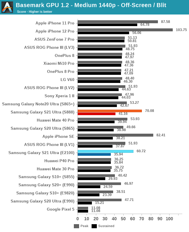
Starting off with Basemark GPU, we’re off to a mixed start. Both the Snapdragon 888 and Exynos 2100 notably outperform their predecessors in terms of peak performance, however their sustained performances on the Galaxy S21 Ultra isn’t too great.
The Exynos 2100 improves dramatically over the Exynos 990 in this regard, however the Snapdragon 888 S21 barely budges the needle against its predecessor, posting roughly the same sustained performance figures as any other Snapdragon 865 device such as the S20 Ultra.
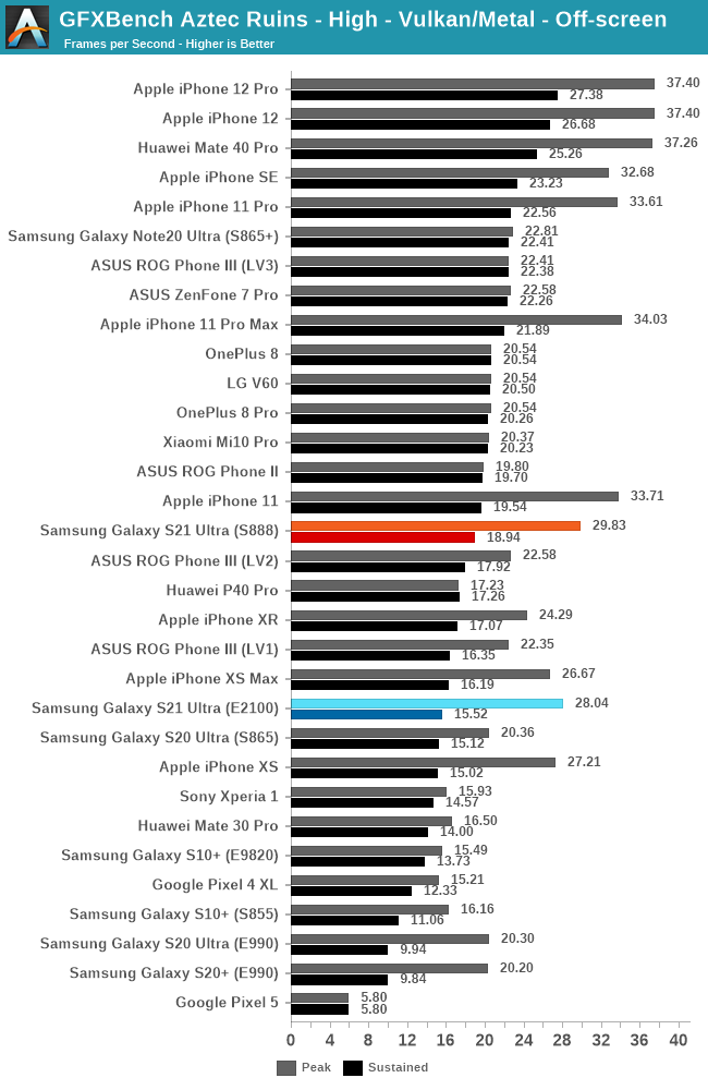
In GFXBench Aztec High, we see a similar story, where peak performance of both phones is much greater than before, however it quickly throttles onto mediocre figures. Again, these are still great improvements for the Exynos, but not so great figures for the Snapdragon 888 S21 Ultra, as it’s posting worse figures than the Note20 Ultra with the Snapdragon 865+.
| GFXBench Aztec High Offscreen Power Efficiency (System Active Power) |
||||
| Mfc. Process | FPS | Avg. Power (W) |
Perf/W Efficiency |
|
| iPhone 12 Pro (A14) 🔥 Throttled | N5 | 28.36 | 3.91 | 7.24 |
| Mate 40 Pro (Kirin 9000) 🔋 Power-Save | N5 | 23.71 | 3.35 | 7.07 |
| iPhone 11 Pro (A13) 🔥 Throttled | N7P | 26.14 | 3.83 | 6.82 |
| Galaxy S21U (Snapdragon 888) 🔥 Throttled | 5LPE | 18.94 | 2.81 | 6.71 |
| iPhone 12 Pro (A14) ❄️ Peak | N5 | 37.40 | 5.57 | 6.64 |
| iPhone 11 Pro (A13) ❄️ Peak | N7P | 34.00 | 6.21 | 5.47 |
| Galaxy S20U (Snapdragon 865) | N7P | 20.35 | 3.91 | 5.19 |
| Mate 40 Pro (Kirin 9000) 🔥 Throttled | N5 | 27.37 | 5.39 | 5.07 |
| iPhone XS (A12) 🔥 Throttled | N7 | 19.32 | 3.81 | 5.07 |
| Reno3 5G (Dimensity 1000L) | N7 | 11.93 | 2.39 | 4.99 |
| Galaxy S21U (Exynos 2100) 🔥 Throttled | 5LPE | 18.55 | 3.73 | 4.96 |
| iPhone XS (A12) ❄️ Peak | N7 | 26.59 | 5.56 | 4.78 |
| Mate 40 Pro (Kirin 9000) ❄️ Peak | N5 | 37.22 | 8.53 | 4.36 |
| ROG Phone III (Snapdragon 865+) | N7P | 22.34 | 5.35 | 4.17 |
| Mate 30 Pro (Kirin 990 4G) | N7 | 16.50 | 3.96 | 4.16 |
| Galaxy S21U (Snapdragon 888) ❄️ Peak | 5LPE | 29.82 | 8.10 | 3.68 |
| Galaxy S21U (Exynos 2100) ❄️ Peak | 5LPE | 28.04 | 7.69 | 3.64 |
| Galaxy S20+ (Exynos 990) | 7LPP | 20.20 | 5.02 | 3.59 |
| Galaxy S10+ (Snapdragon 855) | N7 | 16.17 | 4.69 | 3.44 |
| Galaxy S10+ (Exynos 9820) | 8LPP | 15.59 | 4.80 | 3.24 |
In terms of power and power efficiency, red alert, red alert!
Both the Exynos 2100 and Snapdragon 888 are showcasing outrageous peak power figures around 8W, which are figures that are simply impossible to sustain or dissipate in a phone.
We can see that both chips are way beyond their predecessors points in the frequency/voltages curves as the power efficiency is either outright flat, for the Exynos, or worse than their predecessors, like the Snapdragon – meaning both chips are using exponentially more power to try to drive more performance.
The phones quickly throttle down to below 4W – and fluctuate lower or higher depending on your environmental conditions. I was able to get power measurements for the Exynos around the 4W range (though it throttles down to below that), however for the Snapdragon this wasn’t possible as the phone’s thermal management had a very binomial behaviour of either settling at 3W power or ramping up to 6W, with very little inbetween.
Still, at these different power measurement points, we coincidentally ended up with similar performance – with the Snapdragon 888 here taking the lead in efficiency by 35%.
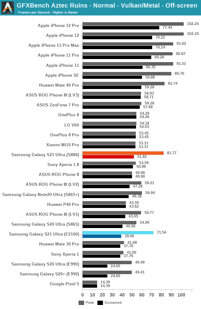
The 1080p variant of Aztec largely looks the same in terms of ranking, with the Exynos 2100 posting a good generational upgrade in sustained performance, while the Snapdragon 888 shows smaller gains.
| GFXBench Aztec Normal Offscreen Power Efficiency (System Active Power) |
||||
| Mfc. Process | FPS | Avg. Power (W) |
Perf/W Efficiency |
|
| iPhone 12 Pro (A14) 🔥 Throttled | N5 | 77.44 | 3.88 | 19.95 |
| iPhone 12 Pro (A14) ❄️ Peak | N5 | 102.24 | 5.53 | 18.48 |
| iPhone 11 Pro (A13) 🔥 Throttled | N7P | 73.27 | 4.07 | 18.00 |
| Galaxy S21U (Snapdragon 888) 🔥 Throttled | 5LPE | 51.81 | 2.93 | 17.67 |
| Mate 40 Pro (Kirin 9000) 🔋 Power-Save | N5 | 53.49 | 3.10 | 17.25 |
| iPhone 11 Pro (A13) ❄️ Peak | N7P | 91.62 | 6.08 | 15.06 |
| iPhone XS (A12) 🔥 Throttled | N7 | 55.70 | 3.88 | 14.35 |
| Galaxy S20U (Snapdragon 865) | N7P | 54.09 | 3.91 | 13.75 |
| iPhone XS (A12) ❄️Peak | N7 | 76.00 | 5.59 | 13.59 |
| Reno3 5G (Dimensity 1000L) | N7 | 27.84 | 2.12 | 13.13 |
| Galaxy S21U (Exynos 2100) 🔥 Throttled | 5LPE | 46.29 | 3.85 | 12.02 |
| Mate 40 Pro (Kirin 9000) 🔥 Throttled | N5 | 63.56 | 5.37 | 11.84 |
| ROG Phone III (Snapdragon 865+) | N7P | 58.77 | 5.34 | 11.00 |
| Mate 40 Pro (Kirin 9000) ❄️ Peak | N5 | 82.74 | 7.95 | 10.40 |
| Mate 30 Pro (Kirin 990 4G) | N7 | 41.68 | 4.01 | 10.39 |
| Galaxy S20+ (Exynos 990) | 7LPP | 49.41 | 4.87 | 10.14 |
| Galaxy S10+ (Snapdragon 855) | N7 | 40.63 | 4.14 | 9.81 |
| Galaxy S21U (Snapdragon 888) ❄️ Peak | 5LPE | 81.77 | 8.40 | 9.73 |
| Galaxy S21U (Exynos 2100) ❄️ Peak | 5LPE | 71.53 | 8.10 | 8.83 |
| Galaxy S10+ (Exynos 9820) | 8LPP | 40.18 | 4.62 | 8.69 |
In terms of power, here’s it’s even higher, with the Snapdragon doing one run at 8.4W of power.
Throttling down, the Snapdragon 888 takes the lead in terms of efficiency as seemingly it has a differently shaped power curve and benefits more at lower frequencies.
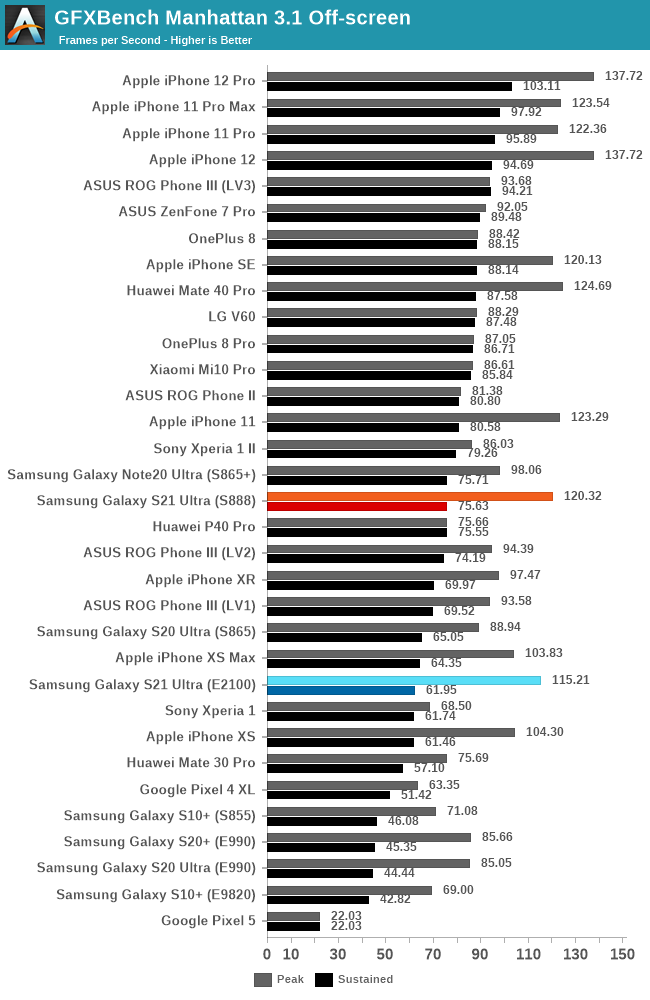
Same story in Manhattan – good upgrades for the Exynos 2100 – although still not very competitive, while the Snapdragon 888 is flat against most other Snapdragon 865 phones.
| GFXBench Manhattan 3.1 Offscreen Power Efficiency (System Active Power) |
||||
| Mfc. Process | FPS | Avg. Power (W) |
Perf/W Efficiency |
|
| iPhone 12 Pro (A14) 🔥 Throttled | N5 | 103.11 | 3.90 | 26.43 |
| Galaxy S21U (Snapdragon 888) 🔥 Throttled | 5LPE | 75.62 | 2.91 | 25.98 |
| iPhone 12 Pro (A14) ❄️ Peak | N5 | 137.72 | 5.63 | 24.46 |
| iPhone 11 Pro (A13) 🔥 Throttled | N7P | 100.58 | 4.21 | 23.89 |
| Mate 40 Pro (Kirin 9000) 🔋 Power-Save | N5 | 95.01 | 4.35 | 21.83 |
| Galaxy S20U (Snapdragon 865) | N7P | 88.93 | 4.20 | 21.15 |
| iPhone 11 Pro (A13) ❄️Peak | N7P | 123.54 | 6.04 | 20.45 |
| iPhone XS (A12) 🔥 Throttled | N7 | 76.51 | 3.79 | 20.18 |
| Reno3 5G (Dimensity 1000L) | N7 | 55.48 | 2.98 | 18.61 |
| Galaxy S21U (Exynos 2100) 🔥 Throttled | 5LPE | 72.66 | 4.04 | 17.98 |
| Mate 40 Pro (Kirin 9000) 🔥 Throttled | N5 | 87.31 | 4.98 | 17.54 |
| iPhone XS (A12) ❄️Peak | N7 | 103.83 | 5.98 | 17.36 |
| ROG Phone III (Snapdragon 865+) | N7P | 93.58 | 5.56 | 16.82 |
| Galaxy S21U (Exynos 2100) ❄️ Peak | 5LPE | 115.20 | 7.62 | 15.11 |
| Mate 40 Pro (Kirin 9000) ❄️Peak | N5 | 124.69 | 8.28 | 15.05 |
| Mate 30 Pro (Kirin 990 4G) | N7 | 75.69 | 5.04 | 15.01 |
| Galaxy S20+ (Exynos 990) | 7LPP | 85.66 | 5.90 | 14.51 |
| Galaxy S10+ (Snapdragon 855) | N7 | 70.67 | 4.88 | 14.46 |
| Galaxy S21U (Snapdragon 888) ❄️ Peak | 5LPE | 120.32 | 8.34 | 14.42 |
| Galaxy S10+ (Exynos 9820) | 8LPP | 68.87 | 5.10 | 13.48 |
| Galaxy S9+ (Snapdragon 845) | 10LPP | 61.16 | 5.01 | 11.99 |
| Mate 20 Pro (Kirin 980) | N7 | 54.54 | 4.57 | 11.93 |
| Galaxy S9 (Exynos 9810) | 10LPP | 46.04 | 4.08 | 11.28 |
| Galaxy S8 (Snapdragon 835) | 10LPE | 38.90 | 3.79 | 10.26 |
| Galaxy S8 (Exynos 8895) | 10LPE | 42.49 | 7.35 | 5.78 |
In terms of power and efficiency, at peak performance the Snapdragon 888 here actually seems to be fare off worse: it’s posting slightly more FPS, however It’s also higher power, reaching up to 8.34W.
Throttling down again shows that the Snapdragon has a steeper power curve and becomes more efficient at lower frequency points. The throttled states of both phones post nearly the same performance, but the Snapdragon does it at 28% lower power.
| GFXBench T-Rex Offscreen Power Efficiency (System Active Power) |
||||
| Mfc. Process | FPS | Avg. Power (W) |
Perf/W Efficiency |
|
| iPhone 12 Pro (A14) 🔥 Throttled | N5 | 260.28 | 4.08 | 63.97 |
| Galaxy S21U (Snapdragon 888) 🔥 Throttled | 5LPE | 172.67 | 2.70 | 63.74 |
| iPhone 11 Pro (A13) 🔥 Throttled | N7P | 289.03 | 4.78 | 60.46 |
| iPhone 12 Pro (A14) ❄️ Peak | N5 | 328.50 | 5.55 | 59.18 |
| iPhone 11 Pro (A13) ❄️ Peak | N7P | 328.90 | 5.93 | 55.46 |
| Galaxy S20U (Snapdragon 865) | N7P | 205.37 | 3.83 | 53.30 |
| Mate 40 Pro (Kirin 9000) 🔥 Throttled | N5 | 147.13 | 2.92 | 50.38 |
| iPhone XS (A12) 🔥 Throttled | N7 | 197.80 | 3.95 | 50.07 |
| Mate 40 Pro (Kirin 9000) 🔋 Power-Save | N5 | 201.85 | 4.10 | 49.22 |
| ROG Phone III (Snapdragon 865+) | N7P | 224.48 | 4.92 | 45.60 |
| iPhone XS (A12) ❄️Peak | N7 | 271.86 | 6.10 | 44.56 |
| Galaxy 10+ (Snapdragon 855) | N7 | 167.16 | 4.10 | 40.70 |
| Galaxy S21U (Exynos 2100) 🔥 Throttled | 5LPE | 153.28 | 3.80 | 40.30 |
| Reno3 5G (Dimensity 1000L) | N7 | 139.30 | 3.57 | 39.01 |
| Mate 40 Pro (Kirin 9000) ❄️ Peak | N5 | 235.04 | 6.11 | 38.46 |
| Galaxy S20+ (Exynos 990) | 7LPP | 199.61 | 5.63 | 35.45 |
| Mate 30 Pro (Kirin 990 4G) | N7 | 152.27 | 4.34 | 35.08 |
| Galaxy S21U (Snapdragon 888) ❄️ Peak | 5LPE | 279.39 | 7.98 | 35.01 |
| Galaxy S9+ (Snapdragon 845) | 10LPP | 150.40 | 4.42 | 34.00 |
| Galaxy 10+ (Exynos 9820) | 8LPP | 166.00 | 4.96 | 33.40 |
| Galaxy S9 (Exynos 9810) | 10LPP | 141.91 | 4.34 | 32.67 |
| Galaxy S8 (Snapdragon 835) | 10LPE | 108.20 | 3.45 | 31.31 |
| Galaxy S21U (Exynos 2100) ❄️ Peak | 5LPE | 237.71 | 8.02 | 29.61 |
| Mate 20 Pro (Kirin 980) | N7 | 135.75 | 4.64 | 29.25 |
| Galaxy S8 (Exynos 8895) | 10LPE | 121.00 | 5.86 | 20.65 |
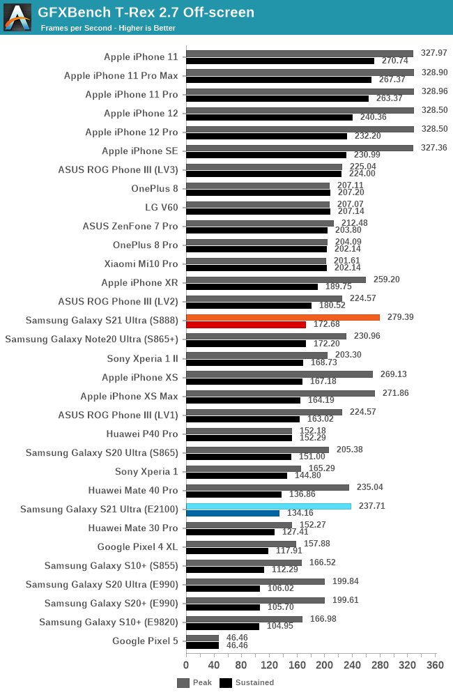
Finally, in T-Rex, the Snapdragon takes a more significant lead in peak performance at the same power, while when throttled down, the Adreno GPU showcases a +50% advantage in perf/W.
Much Too Hot to Handle
I’ll be quite frank with the results of these new SoCs: they’re terrible. Much like smartphone vendors have for years now copied the worst aspects of Apple’s devices, such a dropping headphone jacks and dropping chargers, the SoC vendors this year have now also copied the worst aspect of Apple’s SoCs: extremely high GPU peak power states.
When I tested the Kirin 9000 a few months ago in the Mate 40 Pro I thought that HiSilicon’s choice of turbocharging their massive GPU up to peak power figures of 8W was a very bad choice, but now Qualcomm and Samsung LSI followed up doing the exactly same thing, as if this was a race to the bottom as to who can create the hottest GPU in the market.
As to why the SoC vendors are doing this, it’s very easy to look at the benchmark charts and see the marketing pressure that Apple applies on the rest of the industry, being far ahead of the pack in terms of performance and efficiency. I wouldn’t be surprised if this generation of SoCs have had design decisions impacted by the marketing departments.
Inside devices such as the Galaxy S21 Ultra today – these peak performance states are utterly pointless as they are just impossible to maintain for any reasonable amount of time, as the thermal envelope of the phones really aren’t any different to that of any other device of this form-factor, including the predecessor S20 Ultra.
The Snapdragon 888’s peak performance state is pretty absurd, as at its 840MHz GPU frequency I’ve measured average power of around 11W. This state can’t be maintained for longer than a few seconds before it throttles down to 778 and 738MHz at 9-8W for the rest of the duration of a test on a cold device, before further limiting down due to thermals during prolonged periods. In terms of sustained performance, the S21U’s advantages over the S20U is in the 5-20% range, depending on workload, well below Qualcomm’s proclaimed 35% performance boost. That margin here actually is even smaller against the Snapdragon 865+ Galaxy Note20 Ultra.
I asked Qualcomm to rationalise these high-wattage peak performance points, and the official response was that these were enabled in order to give a higher level of flexibility in terms of higher power gaming phones and higher thermal envelope devices which are able to sustain greater power levels. I know that at least Xiaomi’s Mi 11 will be more aggressive than the S21 Ultra in terms of sustained power levels, at a cost of higher device temperatures. As for gaming phones – the last few generation of those devices have shown little actual physical design differentiation to actually enable higher thermal envelopes, with most of their advantages simply being that they are allowed to get hotter, showing no advantage over “regular” phones which do the same (OnePlus devices, ZenFone 7 Pro for example). The S21 Ultra here has peak skin temperatures of around 46°C with long-term throttling at around 42°C.
For the Exynos 2100 – Samsung LSI’s claim of a 40% performance boost is more credible as this not only refers to the peak performance figures, but can actually also be applied to the sustained performance figures of the phone. It’s actually a tangible and very large upgrade to the Exynos 990 last year, however it needs to be put into context. The peak power figures here have the same negative connotations as on the Snapdragon unit so I won’t repeat myself in that aspect.
In terms of sustained performance, although the Exynos 2100 is a large generational upgrade, it still falls below that of last-generation Snapdragon 865 devices, and naturally also the newer Snapdragon 888. The benchmark figures here also pretty much correspond to the real-world gaming performance of the phones – the Exynos S21 Ultra fared not only worse than the Snapdragon S21 Ultra, but also worse than a Snapdragon S20 Ultra or Note20 Ultra.
The interesting data here is the comparison to Huawei’s Mate 40 Pro with the Kirin 9000 and its gargantuan Mali-G78MP24 GPU – 10 more cores than the Exynos 2100’s configuration. Putting the Mate 40 Pro into power-saving mode will actually cap the maximum GPU frequency and give you reasonable power consumption figures around 4W, which are comparable to what the Exynos 2100 in the S21 Ultra throttles at. We can see that the Kirin’s performance is either superior, lower power, or both, signifying the chip is being notably more efficient than the Exynos 2100. The larger GPU as well as the superior TSMC 5nm node come at play here.
Samsung LSI’s confirmation that they’ll be deploying AMD’s RDNA-based GPU for next-generation flagship SoCs will hopefully mean that the Exynos’ competitive positioning will be quite different next year; however, we shouldn’t expect miracles as the process node differences to Apple’s GPUs will likely still linger on.
Unfortunately, Samsung’s (the mobile division) battery saving mode on the Galaxy S21 doesn’t affect the GPU frequencies at all, unlike Huawei’s PSM, so it doesn’t help at all for the power envelopes or efficiency. I would highly recommend them to introduce such a mechanism here as having burning hot phones really isn’t a great experience while gaming, and the performance will regress to those sustained levels anyhow.
Generally, I see this generation as quite the disappointment when it comes to GPU advancements. Qualcomm likely suffered an efficiency set-back and minor improvements due to the process node shift, and while Samsung LSI has achieved good generational advancements, the Exynos still clearly falls behind due to architectural GPU disadvantages.


123 Comments
View All Comments
serendip - Monday, February 8, 2021 - link
I'm interested in what this means for the SD8cx successor. A 30% increase from using one or two X1 cores would be great, I'm using the SQ2 chip and that's fast enough for typical office tasks. That's still not enough to get within striking range of the M1 or even A14. What the heck is in those Firestorms that makes them so fast?On memory subsystems, what are Qualcomm and Samsung doing wrong compared to Apple and HiSilicon? The M1's memory bandwidth is astonishingly high but that's from using custom parts. HiSilicon is doing a great job using standard ARM interconnects.
Agreed on the stupidly high GPU clocking. The SQ2 has a beefy GPU that performs well but it can get hot even in a large tablet form factor. It's time to stop the marketing departments from forcing engineers to chase pointless metrics.
ikjadoon - Monday, February 8, 2021 - link
>What the heck is in those Firestorms that makes them so fast?A trifecta that I share with people because this question comes up so often.
Technical Part 1: https://www.anandtech.com/show/16226/apple-silicon...
Technical Part 2: https://www.anandtech.com/show/16252/mac-mini-appl...
Consumer + Approachable: https://www.youtube.com/watch?v=3SG5e4z-Ygg
Technical Background + More Approachable: https://www.youtube.com/watch?v=cAjarAgf0nI
As Upscaled wrote, "It's not magic. It's good design." And why don't AMD / Intel have these same good designs? The videos above give thorough answers. For example, the last link explains why everyone cares Firestorm (A14) and Lightning (A13) have an 8-wide decode, which is one of many major "better designs" versus competing Arm & x86 CPUs.
ikjadoon - Monday, February 8, 2021 - link
Uh, wait. Delete. I definitely skipped too much of that one. What on Earth is he going on about 1T vs 1C?~~ Consumer + Approachable: https://www.youtube.com/watch?v=3SG5e4z-Ygg ~~
Wow, I'm a little stunned at how bad this Upscaled video is. The Dev Doc + AnandTech are much more reliable.
Nicon0s - Monday, February 8, 2021 - link
LoL, Engadget.He keeps saying multithreading when he means SMT or Hyperthreading(Intel's version of SMT).
ikjadoon - Monday, February 8, 2021 - link
Yes! Never mind 1T / 1C have shown negligence IPC differences in general computing. 1% at best. Please go test an i5-8600K vs an i7-8700K: one has SMT, one does not. Terrible to see the WCCFTech disinformation cycle reach a mainstream audience so quickly.https://www.anandtech.com/show/16261/investigating...
And then he, out of left field, throws up a Cinebench multi-core score: "See? Intel and Apple are actually very close to each other." But, his comparison was the 4+4 M1 vs an 8C Intel...
I wish I could edit comments. I give up on consumer YouTube videos; I saw his earlier interview with RISC's founders and it seemed halfway decent. I'm a fool.
Archer_Legend - Tuesday, February 9, 2021 - link
Don't be offended but I think that what you posted is completely bs.First of all you are comparing arm64 cpus and x86 cpus, second the arm 64 cores used by apple are very arguably faster than the x86 cores of for example a ryzen cpu.
The second thing which I would want to point out is that about the widht of the pipeline, it is not that apple is a genious or intel and amd are stupid: the x86 architecture was built to have a narrowish pipeline and do more cycles in fact the width of the pipeline in intel and amd cpus is as wide as it gets.
Arm arch on the other end lets you use a wider pipeline, however saying using a narrower or wider pipeline is better or not is pointless because performance comes down to how you organise the cpu around that specific pipeline so....
leledumbo - Monday, February 8, 2021 - link
> What the heck is in those Firestorms that makes them so fast?The same thing since A9 again (CMIIW): super wide decoder + super big cache. Apple isn't stingy when it comes to die size and Apple SoCs are always bigger than Snapdragon on the same generation and process node. 4mm^2 difference is huge when we're talking at nm level. What's weird, Exynos is even bigger but can't match these two. No idea what Samsung put there.
Santoval - Tuesday, February 9, 2021 - link
"What's weird, Exynos is even bigger but can't match these two. No idea what Samsung put there."This is probably due to TSMC having a *far* denser 5nm process node compared to Samsung's process 5nm node. Per the article below TSMC's 5nm node tops at 173 million transistors per mm^2 while Samsung's 5nm node reaches only 126.5 MTr/mm^2 (i.e. barely denser than TSMC's second gen 7nm+ node) due to much more, er, "conservative" design choices (Samsung basically just switched from DDB cells in 7nm to SDB cells; the article explains what that means).
What is often not clear is that the quoted transistor densities of each process node are always the *maximum* transistor densities, not the actual transistor densities used to fab a die. For instance Intel have three different 10nm node variants with three different densities, a low, mid and high density variant (ranging I believe from ~55 million to ~100 million transistors per mm^2). The last one is the only one that has been widely reported, the other two were intended for the tech savvy press and audience.
Each Intel 10nm die has a mix of all three libraries, but each design is (obviously) *fixed* with a precise mix of the three. The desktop parts always have a higher percentage of low density cells because these need to clock higher, and vice versa for the mobile parts. Mobile phones are efficiency focused, so their SoCs have the highest percentage of the highest density variant of each process node that is possible (without hindering performance too much).
That is an additional reason their clocks top at ~3 GHz. Since the two SoCs of the article are both mobile SoCs of an almost identical design we can assume a roughly equivalent percentage of the highest density cells each process node maxes out at. Thus, if all else was being equal (including the same iGPU) Samsung's SoC would have a roughly ~27% larger die than TSMC's SoC. That must be the main reason Samsung kept the cache sizes of the X1 and the A55 cores low.
Santoval - Tuesday, February 9, 2021 - link
p.s. Sorry, I forgot the link to the article :https://semiwiki.com/semiconductor-manufacturers/s...
Santoval - Tuesday, February 9, 2021 - link
p.s.2 I just noticed that the Snapdragon 888 is also fabbed with Samsung's 5nm node. While that rendered the comparison between the two SoCs in my above comment moot the other things I pointed out might have some "academic" value regarding process nodes (I have no away to delete the comment anyway..).