AMD Ryzen 9 5980HS Cezanne Review: Ryzen 5000 Mobile Tested
by Dr. Ian Cutress on January 26, 2021 9:00 AM EST- Posted in
- CPUs
- AMD
- Vega
- Ryzen
- Zen 3
- Renoir
- Notebook
- Ryzen 9 5980HS
- Ryzen 5000 Mobile
- Cezanne
CPU Tests: Microbenchmarks
Core-to-Core Latency
As the core count of modern CPUs is growing, we are reaching a time when the time to access each core from a different core is no longer a constant. Even before the advent of heterogeneous SoC designs, processors built on large rings or meshes can have different latencies to access the nearest core compared to the furthest core. This rings true especially in multi-socket server environments.
But modern CPUs, even desktop and consumer CPUs, can have variable access latency to get to another core. For example, in the first generation Threadripper CPUs, we had four chips on the package, each with 8 threads, and each with a different core-to-core latency depending on if it was on-die or off-die. This gets more complex with products like Lakefield, which has two different communication buses depending on which core is talking to which.
If you are a regular reader of AnandTech’s CPU reviews, you will recognize our Core-to-Core latency test. It’s a great way to show exactly how groups of cores are laid out on the silicon. This is a custom in-house test built by Andrei, and we know there are competing tests out there, but we feel ours is the most accurate to how quick an access between two cores can happen.
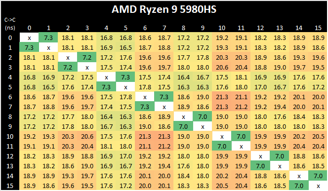
AMD’s move from a dual 4-core CCX design to a single larger 8-core CCX is a key characteristic of the new Zen3 microarchitecture. Beyond aggregating the separate L3’s together for a large single pool in single-threaded scenarios, the new Cezanne-based mobile SoCs also completely do away with core-to-core communications across the SoC’s infinity fabric, as all the cores in the system are simply housed within the one shared L3.
What’s interesting to see here is also that the new monolithic latencies aren’t quite as flat as in the previous design, with core-pair latencies varying from 16.8ns to 21.3ns – probably due to the much larger L3 this generation and more wire latency to cross the CCX, as well as different boost frequencies between the cores. There has been talk as to the exact nature of the L3 slices, whether they are connected in a ring or in an all-to-all scenario. AMD says it is an 'effective' all-to-all, although the exact topology isn't quite. We have some form of mesh with links, beyond a simple ring, but not a complete all-to-all design. This will get more complex should AMD make these designs larger.
Cache-to-DRAM Latency
This is another in-house test built by Andrei, which showcases the access latency at all the points in the cache hierarchy for a single core. We start at 2 KiB, and probe the latency all the way through to 256 MB, which for most CPUs sits inside the DRAM (before you start saying 64-core TR has 256 MB of L3, it’s only 16 MB per core, so at 20 MB you are in DRAM).
Part of this test helps us understand the range of latencies for accessing a given level of cache, but also the transition between the cache levels gives insight into how different parts of the cache microarchitecture work, such as TLBs. As CPU microarchitects look at interesting and novel ways to design caches upon caches inside caches, this basic test proves to be very valuable.
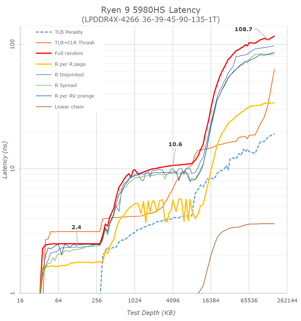
As with the Ryzen 5000 Zen3 desktop parts, we’re seeing extremely large changes in the memory latency behaviour of the new Cezanne chip, with AMD changing almost everything about how the core works in its caches.
At the L1 and L2 regions, AMD has kept the cache sizes the same at respectively 32KB and 512KB, however depending on memory access pattern things are very different for the resulting latencies as the engineers are employing more aggressive adjacent cache line prefetchers as well as employing a brand-new cache line replacement policy.
In the L3 region from 512KB to 16 MB - well, the fact that we’re seeing this cache hierarchy quadrupled from the view of a single core is a major benefit of cache hit rates and will greatly benefit single-threaded performance. The actual latency in terms of clock cycles has gone up given the much larger cache structure, and AMD has also tweaked and changes the dynamic behaviour of the prefetchers in this region.
In the DRAM side of things, the most visible change is again this much more gradual latency curve, also a result of Zen3’s newer cache line replacement policy. All the systems tested here feature LPDDR4X-4266 memory, and although the new Cezanne platform has a slight advantage with the timings, it ends up around 13ns lower latency at the same 128MB test depth point into DRAM, beating the Renoir system and tying with Intel’s Tiger Lake system.
Frequency Ramping
Both AMD and Intel over the past few years have introduced features to their processors that speed up the time from when a CPU moves from idle into a high powered state. The effect of this means that users can get peak performance quicker, but the biggest knock-on effect for this is with battery life in mobile devices, especially if a system can turbo up quick and turbo down quick, ensuring that it stays in the lowest and most efficient power state for as long as possible.
Intel’s technology is called SpeedShift, although SpeedShift was not enabled until Skylake.
One of the issues though with this technology is that sometimes the adjustments in frequency can be so fast, software cannot detect them. If the frequency is changing on the order of microseconds, but your software is only probing frequency in milliseconds (or seconds), then quick changes will be missed. Not only that, as an observer probing the frequency, you could be affecting the actual turbo performance. When the CPU is changing frequency, it essentially has to pause all compute while it aligns the frequency rate of the whole core.
We wrote an extensive review analysis piece on this, called ‘Reaching for Turbo: Aligning Perception with AMD’s Frequency Metrics’, due to an issue where users were not observing the peak turbo speeds for AMD’s processors.
We got around the issue by making the frequency probing the workload causing the turbo. The software is able to detect frequency adjustments on a microsecond scale, so we can see how well a system can get to those boost frequencies. Our Frequency Ramp tool has already been in use in a number of reviews.
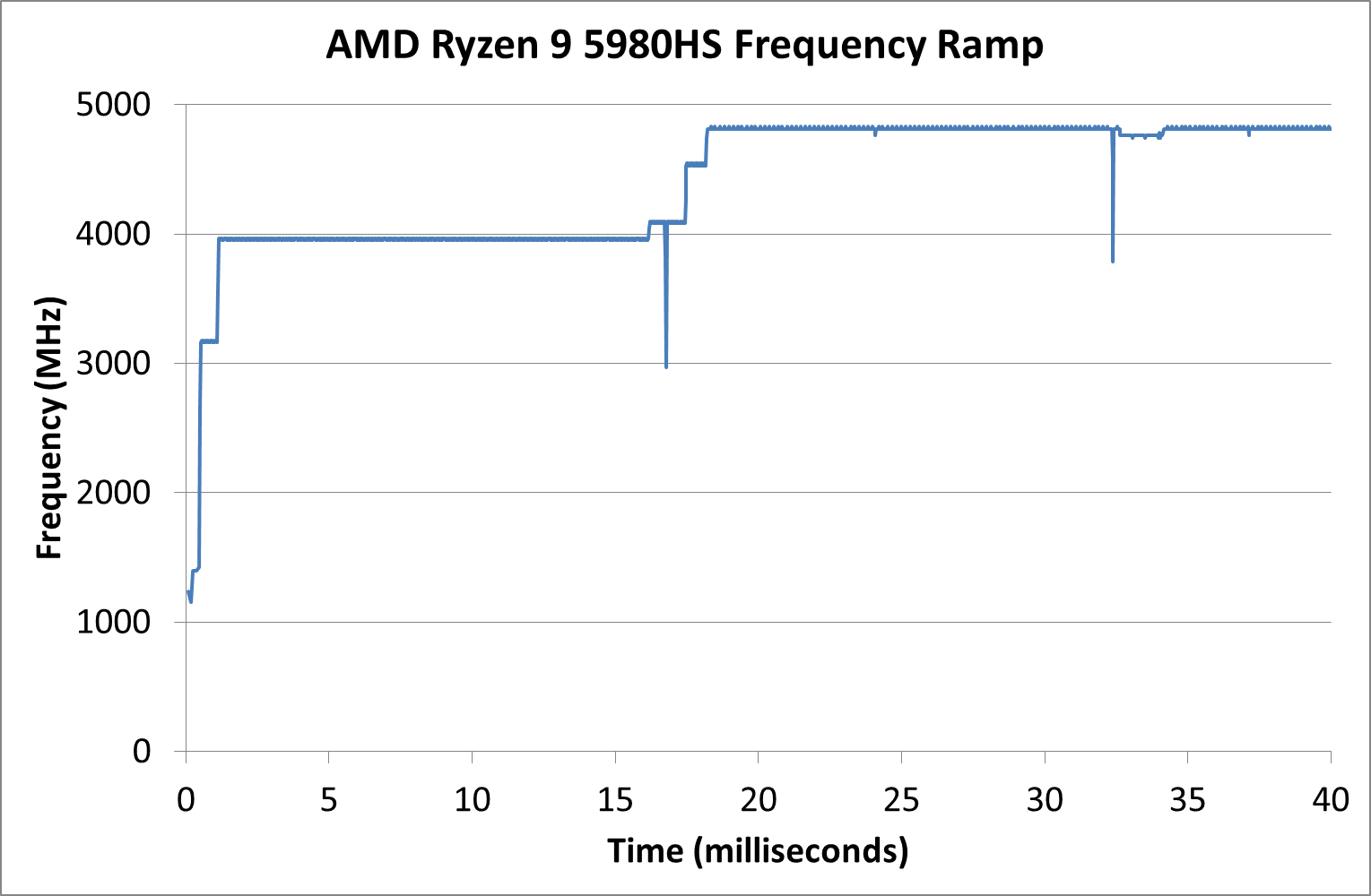
Our frequency ramp showcases that AMD does indeed ramp up from idle to a high speed within 2 milliseconds as per CPPC2. It does take another frame at 60 Hz (16 ms) to go up to the full turbo of the processor mind.


218 Comments
View All Comments
GeoffreyA - Wednesday, January 27, 2021 - link
That would mean more design effort on AMD's part, having APU and non-APU versions. In all likelihood, not worth it to them. Anyhow, these iGPUs work pretty well for older or simpler games. Also, some people might be interested more in the CPU performance (say, for encoding) but would still like to play the odd game now and then.jakky567 - Wednesday, January 27, 2021 - link
For laptops? Yeah, you kinda want integrated graphics for the power savings. I mean, not everyone needs a dedicated gpu too.Ideally you'd get both, but yeah, AMD hasn't made rdna2 in laptops available. You can get Ampere in quite a few though.
oRAirwolf - Tuesday, January 26, 2021 - link
"...as well as a Western Digital SN350 1TB PCIe 3.0 x4 NVMe storage drive."I think you meant an SN530
TheHughMan - Wednesday, January 27, 2021 - link
Using Threadripper model numbers on laptop CPUs can drive unrealistic expectations through the roof.Qasar - Wednesday, January 27, 2021 - link
how is this using threadripper model numbers ?yeeeeman - Wednesday, January 27, 2021 - link
Barely faster than last gen...AMD has hit the process limitation wall it seems, they need 5nm.
ABR - Wednesday, January 27, 2021 - link
Thank you for including a compile benchmark, finally!Retycint - Wednesday, January 27, 2021 - link
Apparently, on Chinese forums there have been reports of abnormally slow L3 cache speeds - 150 GB/s instead of 600GB/s, tested via AIDA64. Not sure about the exact numbers, but the actual speeds were supposedly much lower than the theoretical speeds. Is there any indication of this occurring?Oxford Guy - Wednesday, January 27, 2021 - link
'1 TB NVMe SSD'Underwhelming, considering my 2013 Macbook Pro has a stock 1 TB SSD.
Kuhar - Wednesday, January 27, 2021 - link
LOL, what a liar. Everyone can check on google what the stock MBP 2013 was. To inform you - stock was 256 gb. Besides that - if all you think about is big size, you will never find a GF.