Qualcomm Details The Snapdragon 888: 3rd Gen 5G & Cortex-X1 on 5nm
by Andrei Frumusanu on December 2, 2020 10:00 AM EST- Posted in
- Mobile
- Qualcomm
- Smartphones
- SoCs
- 5G
- Cortex A78
- Cortex X1
- Snapdragon 888
Triple ISPs: Concurrent Triple-Camera Usage
Interestingly enough, during yesterday’s keynote event, Qualcomm described themselves as a camera company, which is a funny way to see things, but actually somewhat makes sense given the large leaps in smartphone camera capture capabilities over the recent years.
The new Snapdragon 888 pushes the envelope in terms camera abilities by adding a whole new independent third ISP to the SoC, allowing the SoC to now run three independent camera modules concurrently, opening up new use cases for vendors and camera applications.

The new triple-ISP architecture now increases the overall pixel processing throughput by 35% to 2.7Gigapixels/s, allowing for concurrent usage of up to three 28MP sensors with zero shutter lag captures. Alternatively, you can use a combination of 64+25MP sensors with ZSL, or a single 84MP sensor with ZSL. There’s still also support for ultra-high-resolution sensors up to 200MP, but image captures here don’t support ZSL.
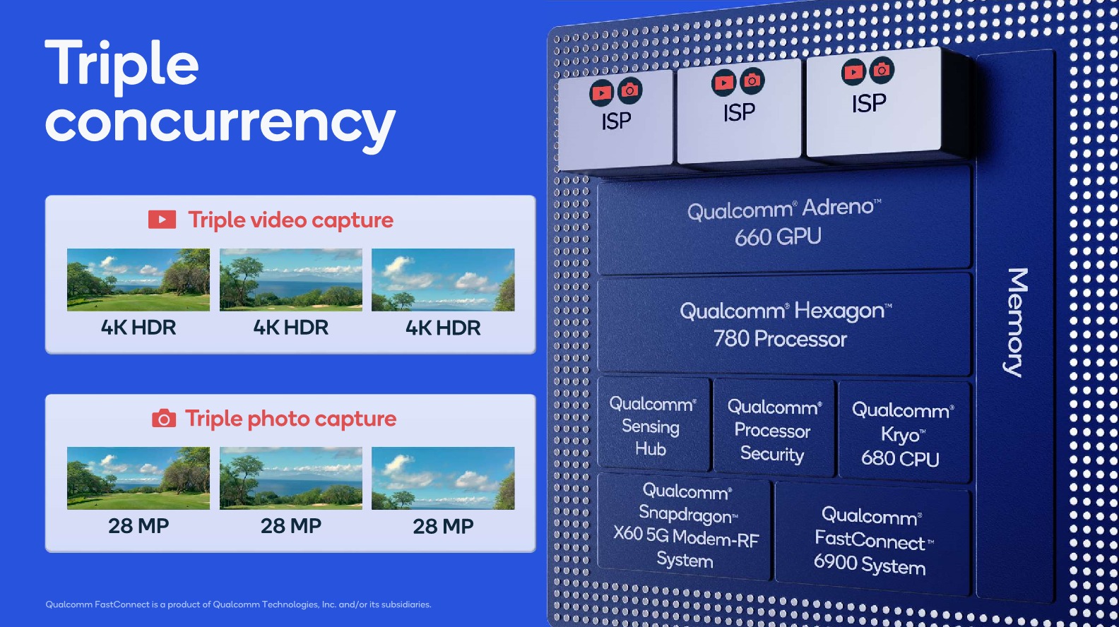
Allowing concurrent captures of three sensors now allows for the holy trifecta of ultra-wide-angle, wide-angle and telephoto modules to capture a scene at the same time, allowing for more interesting use-cases such as image stitching and image fusion to happen to seamlessly.
One interesting capability that Qualcomm was advertising is triple-stream 4K HDR video recording. That’s a bit of an odd-ball use-case as I do wonder about the practical benefits, but I do at least hope that the new triple ISP system allows for more seamless switching and zooming in and out between the various camera modules during video recording.
Video recording capabilities this year don’t seem to have changed, compared to the Snapdragon 865. This means 4K120 or 8K30 are still the peak capture modes, supporting also slow-motion of 720p960. Formats are also unchanged, with HEVC encoding in HDR formats such as HDR10+ or Dolby Vision being supported.
AV1 decoding didn’t make the cut this year unfortunately, which means wide-spread adoption in mobile for the codec will be delayed for another year.
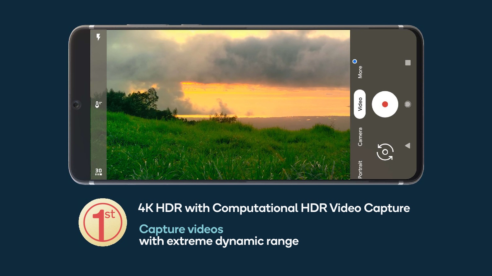
While the video encoding formats haven’t changed, the image processing capabilities for HDR capture has. Thanks to the new ISPs and the raw performance throughput, the new Snapdragon 888 will be able to capture 4K HDR footage with the more advanced computational HDR processing being applied on each and every frame of the video.

Qualcomm claims that the new ISP in the Snapdragon 888 is the first to support new next-generation staggered HDR sensors.
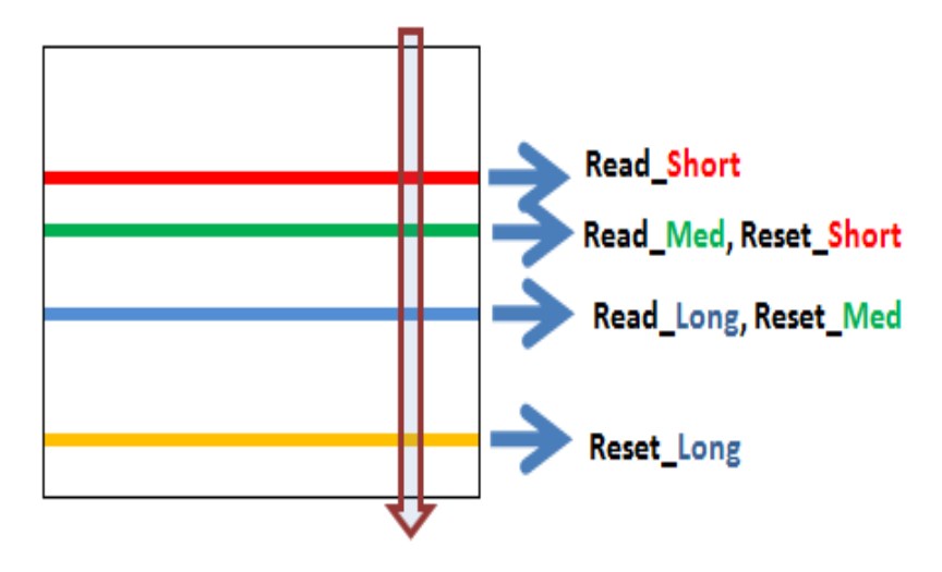
Source: OmniVision
These are sensors that can have multiple rolling shutters, meaning sensor line readouts, active at the same time on the sensor. Instead of taking multiple exposures one at a time sequentially by scanning out the sensor matrix from start to finish, the sensor will start another exposure immediately after the completed line read-out, reducing the time in-between exposures greatly. This should allow for significant less motion ghosting between the exposures and a sharper resulting recombined HDR image capture than current generation sensors which only have a single active line readout on the sensor.
While we haven’t actually heard of such sensors from Samsung or Sony yet, Qualcomm is adamant that we’ll be seeing smartphones in 2021 employing this new technology.

A further improvement for still-picture captures is the advancement of the new multi-frame noise reduction engines inside of the ISPs. It’s said that the quality of the noise reduction has been improved this generation, allowing for even better low-light captures with the native capture mode (no computational photography).


123 Comments
View All Comments
dudedud - Wednesday, December 2, 2020 - link
If the Vivo (V2056A) GB's scores are legit, this implementation of the X1 will be much more close to A12 than to the A13.abufrejoval - Thursday, December 3, 2020 - link
I'd say they design their SoC to suit their usage. And that is a mixed bag full of compromises, matching what people are actually doing on these devices. Very little of that is HPC.The single X1 is for all that fat single-threaded desktop-class browser code out there, that only gets tolerable response times on a 4GHz Pentium 4, but hopefully won't run longer than a couple hundred milliseconds, because an X1 core simply can't run 24x7 on a mobile power budget.
Mobile games better run on the efficiency cores mainly (apart from the GPU), with perhaps short bursts on the power cores, because otherwise not even an hour worth of game time may be possible on a single charge (or without burning your fingers).
In short, don't expect all of these resources used at full capacity for any extended time. Instead these SoCs become a computing appliance farm with specialists for many different tasks, designed to do very little to nothing most of the time and as aesthetically pleasing inside as any SME server room that evolved with the business for 20 years.
To ask for a revolutionary design on a new process from a different fab is perhaps asking just a little bit too much, especially when they need to sell another generation next year.
For such a bad job I am seriously considering that the 888 may be enough of an upgrade over my current 855 to consider, once they sell these devices at reasonable prices (~€500) and with LinageOS support late 2021 or early 2022 with the 895's imminent arrival.
Honestly I've stopped asking for more smartphone computing power since the 820, been perfectly happy with energy effiency since the 835 and been waiting for a proper desktop mode since the first DeX on an 800.
It's hard to sell more when the need doesn't really grow or you can have 500 Watts of desktop power any time you sit done for something serious.
eastcoast_pete - Wednesday, December 2, 2020 - link
As for the choice of Samsung's 5 nm LPE for the manufacturing, I suspect it's not just TSMC's capacity that made QC go Sammy. My guess is that Samsung fabbed it for less - that simple. Sort of why NVIDIA chose Samsung's 8 nm for Ampere; they did it for less.abufrejoval - Thursday, December 3, 2020 - link
With China flexing its muscle over Taiwan, Korea may be more attractive in other ways, too.Then I wonder if the 5nm node on Samsung may actually be faster from start to finish with EUV replacing all those multi-masking and multi-patterning steps...
trivik12 - Wednesday, December 2, 2020 - link
Thanks for the detailed article. Did Qualcomm go with Samsung as they will be taking process leadership in the near future with 1st GAAFET implementation in 2023. It would be good to see where Samsung 5nm is relative to TSMC.Looking at improvements from process and architecture, I feel even ARM is close to hitting the wall.
brucethemoose - Wednesday, December 2, 2020 - link
IDK about that. The schedule is *far* from set in stone, with how extreme the physics are.tkSteveFOX - Wednesday, December 2, 2020 - link
I think ARM wants to keep everyone out of reach of Apple's performance dominance.A55 is vastly inferior to the last 3 gens of small cores Apple has used.
X1 is decent but seeing just a single core in there isn't great.
Not using 8mb cache is purely driven by greed. It will make the chips cost higher and that's why QC aren't doing it, there are substantial gains from using more cache on a CPU in heavy workloads.
All these companies want to make money, so they cut costs of their chips and that's why Android will always be behind iOS.
Apple gives you the most bleeding edge stuff without sacrificing on the chip.
id4andrei - Wednesday, December 2, 2020 - link
That is because QC has to sell these chips to OEMs that have to be able to afford them. Apple doesn't have to sell to no one. They have high margins to justify their investment in performance beyond the scope of Xiaomi, LG, Samsung.melgross - Wednesday, December 2, 2020 - link
ARM doesn’t care about that. They sell designs that are good enough to make them enough money to make a good profit and allow for further work. It’s up to the OEMs to make the changes allowed through the design license to make some improvements. Failing that, companies can get an architectural license as Apple and a few others do, which lets them design cores and subsystems from scratch.Both Qualcomm and Samsung tried that for a few years, but failed to come up with good designs. So they went back to licensing designs from ARM.
Silver5urfer - Wednesday, December 2, 2020 - link
SD820 is not a failure, it was a full custom design which was not a disaster it was superb and even had the IPC speed higher than 835, that's where all this Kryo started. Then Qcomm moved all of their engg arch teams to Centriq the ever famous most powerful ARM server processor, they axed it even after putting so much R&D in that with Cloudflare marketing. Since then Qcomm never made any custom cores. Only Samsung did with ambitious aims but failed to optimize it for the smartphone.And in the end it doesn't even matter, because phones are going to be on parity with A14. Just looking and gaming performance and application performance tests which are real world shows 865 is not even that far vs A14 in some aspects. And Qcomm is putting money where it matters - GPU and 5G.