Qualcomm Details The Snapdragon 888: 3rd Gen 5G & Cortex-X1 on 5nm
by Andrei Frumusanu on December 2, 2020 10:00 AM EST- Posted in
- Mobile
- Qualcomm
- Smartphones
- SoCs
- 5G
- Cortex A78
- Cortex X1
- Snapdragon 888
Triple ISPs: Concurrent Triple-Camera Usage
Interestingly enough, during yesterday’s keynote event, Qualcomm described themselves as a camera company, which is a funny way to see things, but actually somewhat makes sense given the large leaps in smartphone camera capture capabilities over the recent years.
The new Snapdragon 888 pushes the envelope in terms camera abilities by adding a whole new independent third ISP to the SoC, allowing the SoC to now run three independent camera modules concurrently, opening up new use cases for vendors and camera applications.

The new triple-ISP architecture now increases the overall pixel processing throughput by 35% to 2.7Gigapixels/s, allowing for concurrent usage of up to three 28MP sensors with zero shutter lag captures. Alternatively, you can use a combination of 64+25MP sensors with ZSL, or a single 84MP sensor with ZSL. There’s still also support for ultra-high-resolution sensors up to 200MP, but image captures here don’t support ZSL.
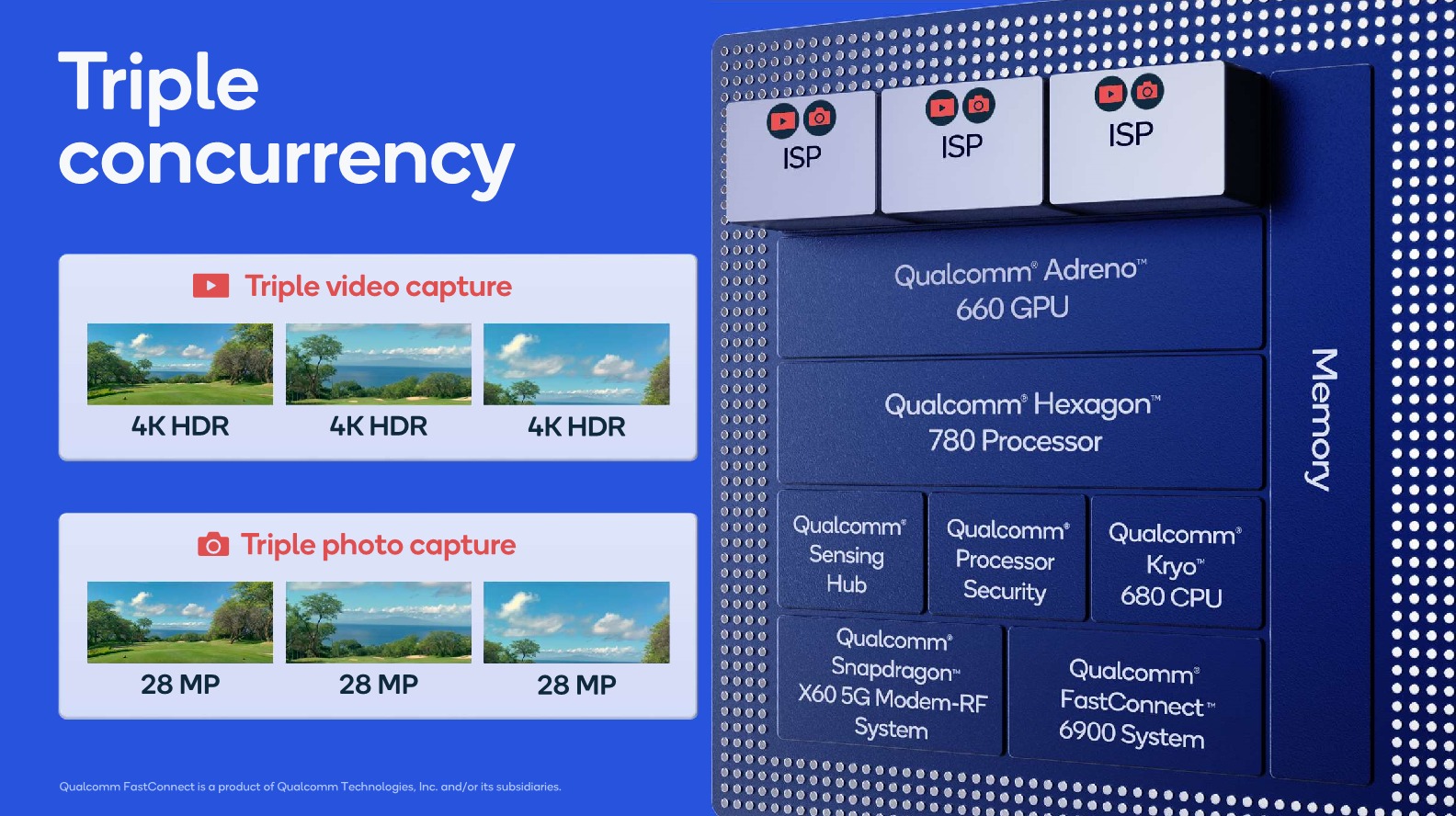
Allowing concurrent captures of three sensors now allows for the holy trifecta of ultra-wide-angle, wide-angle and telephoto modules to capture a scene at the same time, allowing for more interesting use-cases such as image stitching and image fusion to happen to seamlessly.
One interesting capability that Qualcomm was advertising is triple-stream 4K HDR video recording. That’s a bit of an odd-ball use-case as I do wonder about the practical benefits, but I do at least hope that the new triple ISP system allows for more seamless switching and zooming in and out between the various camera modules during video recording.
Video recording capabilities this year don’t seem to have changed, compared to the Snapdragon 865. This means 4K120 or 8K30 are still the peak capture modes, supporting also slow-motion of 720p960. Formats are also unchanged, with HEVC encoding in HDR formats such as HDR10+ or Dolby Vision being supported.
AV1 decoding didn’t make the cut this year unfortunately, which means wide-spread adoption in mobile for the codec will be delayed for another year.
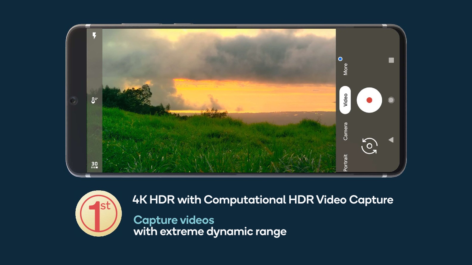
While the video encoding formats haven’t changed, the image processing capabilities for HDR capture has. Thanks to the new ISPs and the raw performance throughput, the new Snapdragon 888 will be able to capture 4K HDR footage with the more advanced computational HDR processing being applied on each and every frame of the video.

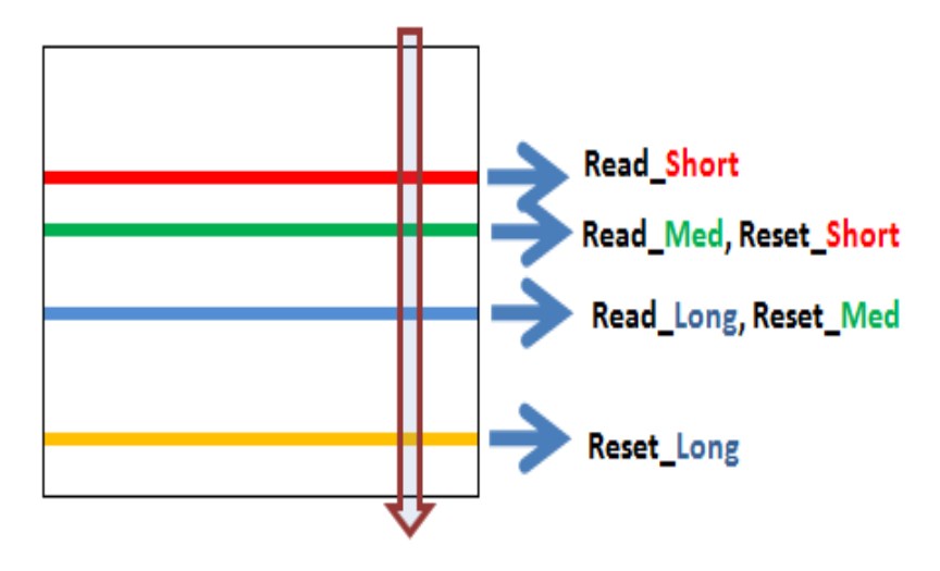
Qualcomm claims that the new ISP in the Snapdragon 888 is the first to support new next-generation staggered HDR sensors.
Source: OmniVision
These are sensors that can have multiple rolling shutters, meaning sensor line readouts, active at the same time on the sensor. Instead of taking multiple exposures one at a time sequentially by scanning out the sensor matrix from start to finish, the sensor will start another exposure immediately after the completed line read-out, reducing the time in-between exposures greatly. This should allow for significant less motion ghosting between the exposures and a sharper resulting recombined HDR image capture than current generation sensors which only have a single active line readout on the sensor.
While we haven’t actually heard of such sensors from Samsung or Sony yet, Qualcomm is adamant that we’ll be seeing smartphones in 2021 employing this new technology.

A further improvement for still-picture captures is the advancement of the new multi-frame noise reduction engines inside of the ISPs. It’s said that the quality of the noise reduction has been improved this generation, allowing for even better low-light captures with the native capture mode (no computational photography).


123 Comments
View All Comments
ZolaIII - Wednesday, December 2, 2020 - link
Well based on the QC claims, 20% more power efficient = same number of GPU clusters and same alignment as the power saving is from process improvement, they made a new pipeline to include additional functions but fundamental blocks remain unchanged (actually ALU's didn't change from Ati days).This is just based on my assumptions and logic. Upon which I don't think it's enough to be stated as new gen.
I don't have problem with numerology including additional make believes tied to the name change, at least that's not a snake oil like the rest.
Given in mind rest of the story (trade wars) actually the QC naming thing is pathetic.
Who ever makes a real flagship SoC (not saying on the die size), even if based on reference IP's based upon 5 nm TSMC has the opportunity to rip this abomination without to much hustle.
Raqia - Wednesday, December 2, 2020 - link
Transistor count and die size haven't been revealed yet; I have my doubts many other companies could integrate all those subsystems with the PPA that Qualcomm achieves. Even Apple doesn't get there as they don't integrate a modem which is far far trickier than you might expect.ZolaIII - Wednesday, December 2, 2020 - link
Well you are right about that (modem, RF and cetera) and thing's won't get better any time soon, call it democracy.Rest is IP license available. If you raise a bar to actual manufacturers (in their own menagement) list goes to none as ironically Samsung is by far most adequate. I guess things will get boring until GAA.
melgross - Wednesday, December 2, 2020 - link
Apple hasn’t been allowed to integrate a modem. It’s likely that a major reason they bought Intel’s work is so that they can have their own, so that they can do that. But Apple seems to have no problems with efficiency, even with an external modem. I suspect that it’s the Android OSs known efficiency problems, among others, such as the requirement for double the RAM, that’s causing these problems, which is why those phones require batteries that are so much larger.Raqia - Wednesday, December 2, 2020 - link
It's a fallacy that an external modem is any less power efficient than an on SoC one, and in fact fab process can be further optimized for a totally separate modem die which really does have different requirements than CPUs and GPUs. The reason Qualcomm, Samsung, Mediatek and Huawei do it is to reduce cost and complexity. Apple simply doesn't the IP necessary and the purchase of Intel's money losing unit was primarily for IP, some talent rather than design or implementation; it still won't get them a competitive modem in house for several years to come.ZolaIII - Thursday, December 3, 2020 - link
It's a fact how it isn't a one peace to start with. RF analog-mixed part & processesing part which can be integrated. RF part didn't progress regarding it's manufacturing processes in very, very long time & in best case scenario is built upon SOI. In the world of mobile SoC high density libs are commonly used for everything already (excluding analogue, MOSFET's and cetera of course).KusheYemi - Wednesday, December 2, 2020 - link
Qualcomm updated their processor the right way. They improved all of the main day to day functions that ordinary people use frequently. Tech savvy people might be disappointed about the raw compute power but the SD865 was already great.halcyon - Wednesday, December 2, 2020 - link
If they wanted to improve the day-to-day, they would have made it much more power efficient and replaced those ageing A55 cores that are used for mosts daily simple tasks.melgross - Wednesday, December 2, 2020 - link
Great compared to what, other mediocre SoCs?The Hardcard - Wednesday, December 2, 2020 - link
I don’t know why people only see great or horrible with nothing in between. This is a good competitive chip - only people desperately aching for someone to overtake Apple can be seriously disappointed.The single X1 is a solution to having good singlethread speed and the UI responsiveness that comes with that while giving good multicore combined with efficiency. Is it the best solution? I don’t know, but it’s not a bad one.
The clock speed is interesting however. I have to think that there are process limitations there. ARM targeted 3 GHz, which would’ve given it some floating point wins over the A13 based on Andrei‘s estimates. The 5% shortfall will put them pretty squarely behind the A13, I’m sure they wouldn’t have excepted that unless they had no choice.