Apple Announces The Apple Silicon M1: Ditching x86 - What to Expect, Based on A14
by Andrei Frumusanu on November 10, 2020 3:00 PM EST- Posted in
- Apple
- Apple A14
- Apple Silicon
- Apple M1
Apple Shooting for the Stars: x86 Incumbents Beware
The previous pages were written ahead of Apple officially announcing the new M1 chip. We already saw the A14 performing outstandingly and outperforming the best that Intel has to offer. The new M1 should perform notably above that.
We come back to a few of Apple’s slides during the presentations as to what to expect in terms of performance and efficiency. Particularly the performance/power curves are the most detail that Apple is sharing at this moment in time:
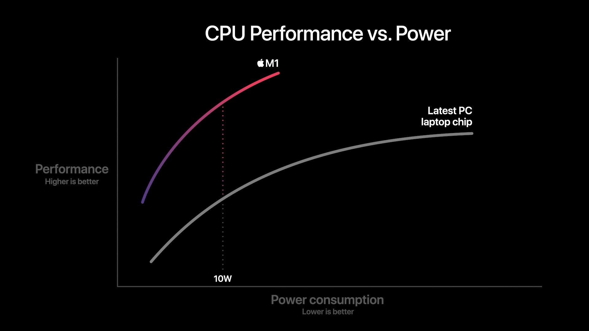
In this graphic, Apple showcases the new M1 chip featuring a CPU power consumption peak of around 18W. The competing PC laptop chip here is peaking at the 35-40W range so certainly these are not single-threaded performance figures, but rather whole-chip multi-threaded performance. We don’t know if this is comparing M1 to an AMD Renoir chip or an Intel ICL or TGL chip, but in both cases the same general verdict applies:
Apple’s usage of a significantly more advanced microarchitecture that offers significant IPC, enabling high performance at low core clocks, allows for significant power efficiency gains versus the incumbent x86 players. The graphic shows that at peak-to-peak, M1 offers around a 40% performance uplift compared to the existing competitive offering, all whilst doing it at 40% of the power consumption.
Apple’s comparison of random performance points is to be criticised, however the 10W measurement point where Apple claims 2.5x the performance does make some sense, as this is the nominal TDP of the chips used in the Intel-based MacBook Air. Again, it’s thanks to the power efficiency characteristics that Apple has been able to achieve in the mobile space that the M1 is promised to showcase such large gains – it certainly matches our A14 data.
Don't forget about the GPU
Today we mostly covered the CPU side of things as that’s where the unprecedented industry shift is happening. However, we shouldn’t forget about the GPU, as the new M1 represents Apple’s first-time introduction of their custom designs into the Mac space.
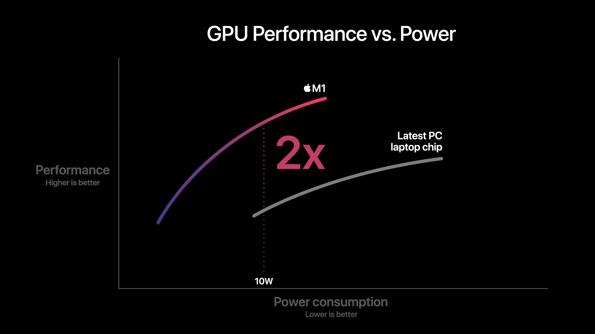
Apple’s performance and power efficiency claims here are really lacking context as we have no idea what their comparison point is. I won’t try to theorise here as there’s just too many variables at play, and we don’t know enough details.
What we do know is that in the mobile space, Apple is absolutely leading the pack in terms of performance and power efficiency. The last time we tested the A12Z the design was more than able to compete and beat integrated graphics designs. But since then we’ve seen more significant jumps from both AMD and Intel.
Performance Leadership?
Apple claims the M1 to be the fastest CPU in the world. Given our data on the A14, beating all of Intel’s designs, and just falling short of AMD’s newest Zen3 chips – a higher clocked Firestorm above 3GHz, the 50% larger L2 cache, and an unleashed TDP, we can certainly believe Apple and the M1 to be able to achieve that claim.
This moment has been brewing for years now, and the new Apple Silicon is both shocking, but also very much expected. In the coming weeks we’ll be trying to get our hands on the new hardware and verify Apple’s claims.
Intel has stagnated itself out of the market, and has lost a major customer today. AMD has shown lots of progress lately, however it’ll be incredibly hard to catch up to Apple’s power efficiency. If Apple’s performance trajectory continues at this pace, the x86 performance crown might never be regained.


644 Comments
View All Comments
pcordes - Thursday, November 19, 2020 - link
Thanks for the microarchitectural testing and details!However, some current Intel / AMD numbers you use for comparison aren't right. (Also, your ROB-size and load/store buffers graphs are missing labels on the vertical axis; I assume that's time or cycles or something with.)
Intel since Skylake has 5-wide legacy decode (up from 4-wide in Haswell) and 6-wide fetch from the decoded-uop cache. (The issue/rename stage is still only 4-wide in Skylake, but widened to 5 in Ice Lake. Being wider earlier in the front-end can catch up after stalls, letting buffers between stages hide bubbles) https://en.wikichip.org/wiki/intel/microarchitectu...
https://en.wikichip.org/wiki/intel/microarchitectu...
(The decoders can also macro-fuse a cmp/jcc branch into 1 uop, so max decode throughput is actually 7 x86 instructions per clock, into 5 uops.)
AMD Zen 2 can decode up to 4 x86 instructions per clock. (Not sure if that includes fusion of cmp/jcc or not). This is probably where you got your 4-wide number that you claimed applied to Intel. But that's just legacy-decode. Most code spends a lot of time in non-huge loops, and they can run from the uop cache. Zen 2's decoded-uop cache can produce up to 8 uops/clock.
https://en.wikichip.org/wiki/amd/microarchitecture...
The actual bottleneck for sending instructions into the out-of-order back-end is the issue/rename stage as usual: 6 uops, but I think those can only come from up to 5 x86 instructions. I thought I remembered reading that Zen 1 could only sustain 6 uops / clock when running code that included some AVX 256-bit instructions or other 2-uop instructions. Maybe that changed with Zen2 (where most 256-bit SIMD instructions are still 1 uop), I don't have an AMD system to test on, and stuff like https://uops.info/ only tests throughput of single instructions, not a mix of integer, FP, and/or loads/store.
Anyway, Zen's front-end is at least 5-wide, and 6-wide for at least some purposes.
---
You seem to be saying M1 can do 4 FADDs *and* 4 FMULs in the same cycle. That doesn't make any sense with "only" 4 FP execution units. Perhaps you mean 4 FMAs per cycle? Or can each execution unit really accept 2 instructions in the same clock cycle, like Pentium 4's double-pumped integer ALUs?
That's only twice the throughput of Haswell/Skylake, or the same throughput if you take vector width into account, assuming Apple M1 doesn't have ARM SVE for wider vectors.
(Skylake has FMA units on ports 0 and 1, each 256-bit wide. FP mul / add also run on those same units, all with 4-cycle latency. So using FMAs instead of `vaddps` or `vmulps` gives Skylake twice the FLOPS because an FMA counts as two FLOPs, despite being a single operation for the pipeline.)
Zen2 runs vaddps on ports FP2 / FP3, and vmulps or vfma...ps on FP0 / FP1. So it can sustain 2/clock FADD *and* 2/clock FMUL/FMA, unlike Skylake that can only do a total of 2 FP ops per cycle. (Both with any width from scalar to 256-bit). Zen1 has the same port allocations, but the execution units are only 128 bits wide. (Numbers from https://uops.info/)
https://en.wikichip.org/wiki/amd/microarchitecture... doesn't indicate any more FMA or SIMD FP mul/add throughput, except reduced competition from FP store and FP->int.
You weren't looking at actual legacy x87 `fadd` / `fmul` instruction mnemonics were you? Modern x86 does FP math using SSE / AVX instructions like scalar addsd / mulsd (sd = scalar double), with fewer execution units for legacy 80-bit x87. (Unfortunately FMA isn't baseline, only available as an extension, unlike with AArch64.)
LYP - Sunday, May 23, 2021 - link
I'm happy that I'm not the only one who thinks there is something wrong here ...peevee - Wednesday, December 9, 2020 - link
"Intel has stagnated itself out of the market, and has lost a major customer today."A decade+ concentrating on "diversity and inclusion" vs competency can do that to you. Their biggest problem today might be the Portland location and culture.
IntoGraphics - Wednesday, December 16, 2020 - link
<blockquote>"If Apple’s performance trajectory continues at this pace, the x86 performance crown might never be regained."</blockquote>If Apple's performance trajectory does continue at this pace, the x86 performance crown will be irrelevant.