A Broadwell Retrospective Review in 2020: Is eDRAM Still Worth It?
by Dr. Ian Cutress on November 2, 2020 11:00 AM ESTBroadwell with eDRAM: Still Has Gaming Legs
As we crossover into the 2020s era, we now have more memory bandwidth from DRAM than a processor in 2015. Intel's Broadwell processors were advertised as having 128 megabytes of 'eDRAM', which enabled 50 GiB/s of bidirectional bandwidth at a lower latency of main memory, which ran only at 25.6 GiB/s. Modern processors have access to DDR4-3200, which is 51.2 GiB/s, and future processors are looking at 65 GiB/s or higher.
At this time, it is perhaps poignant to take a step back and understand the beauty of having 128 MiB of dedicated silicon for a singular task.
Intel’s eDRAM enabled Broadwell processors accelerated a significant number of memory bandwidth and memory latency workloads, in particular gaming. What eDRAM has enabled in our testing, even if we bypass the now antiquated CPU performance, is surprisingly good gaming performance. Most of our CPU gaming tests are designed to enable a CPU-limited scenario, which is exactly where Broadwell can play best. Our final CPU gaming test is a 1080p Max scenario where the CPU matters less, but there still appears to be good benefits from having an on-die DRAM and that much lower latency all the way out to 128 MiB.
There have always been questions around exactly what 128 MiB of eDRAM cost Intel to produce and supply to a generation of processors. At launch, Intel priced the eDRAM versions of 14 nm Broadwell processors as +$60 above the non-eDRAM versions of 22 nm Haswell equivalents. There are arguments to say that it cost Intel directly somewhere south of $10 per processor to build and enable, but Intel couldn’t charge that low, based on market segmentation. Remember, that eDRAM was built on a mature 22 nm SoC process at the time.
As we move into an era where AMD is showcasing its new ‘double’ 32 MiB L3 cache on Zen 3 as a key part of their improved gaming performance, we already had 128 MiB of gaming acceleration in 2015. It was enabled through a very specific piece of hardware built into the chip. If we could do it in 2015, why can’t we do it in 2020?
What about HBM-enabled eDRAM for 2021?
Fast forward to 2020, and we now have mature 14 nm and 7 nm processes, as well as a cavalcade of packaging and eDRAM opportunities. We might consider that adding 1-2 GiB of eDRAM to a package could be done with high bandwidth connectivity, using either Intel’s embedded multi-die technology or TSMC’s 3DFabric technology.
If we did that today, it could arguably be just as complex as what it was to add 128 MiB back in 2015. We now have extensive EDA and packaging tools to deal with chiplet designs and multi-die environments.
So consider, at a time where high performance consumer processors are in the realm of $300 up to $500-$800, would customers consider paying +$60 more for a modern high-end processor with 2 gigabytes of intermediate L4 cache? It would extend AMD’s idea of high-performance gaming cache well beyond the 32 MiB of Zen 3, or perhaps give Intel a different dynamic to its future processor portfolio.
As we move into more a chiplet enabled environment, some of those chiplets could be an extra cache layer. However, to put some of this into perspective.
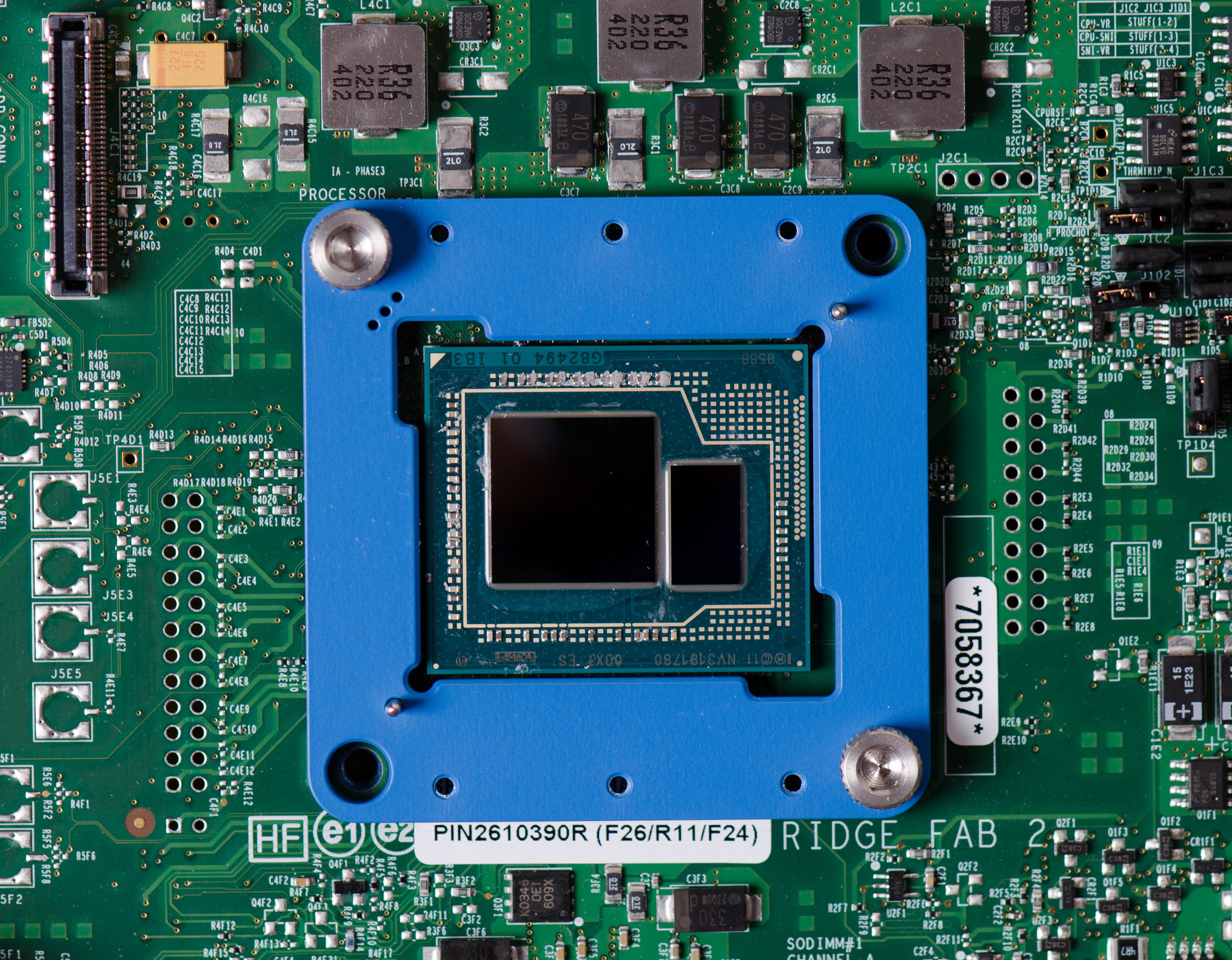
- Intel's Broadwell's 128 MiB of eDRAM was built (is still built) on Intel's 22nm IO process and used 77 mm2 of die area.
- AMD's new RX 6000 GPUs use '128 MiB' of 7nm Infinity Cache SRAM. At an estimated 6.4 billion transistors, or 24% of the 26.8 billion transistors and ~510-530mm2 die, this cache requires a substantial amount of die area, even on 7nm.
This would suggest that in order for future products to integrate large amounts of cache or eDRAM, then layered solutions will need to be required. This will require large investment in design and packaging, especially thermal control.
Many thanks to Dylan522p for some minor updates on die size and pointing out that the same 22nm eDRAM chip is still in use today with Apple's 2020 base Macbook Pro 13.


120 Comments
View All Comments
Leeea - Monday, November 2, 2020 - link
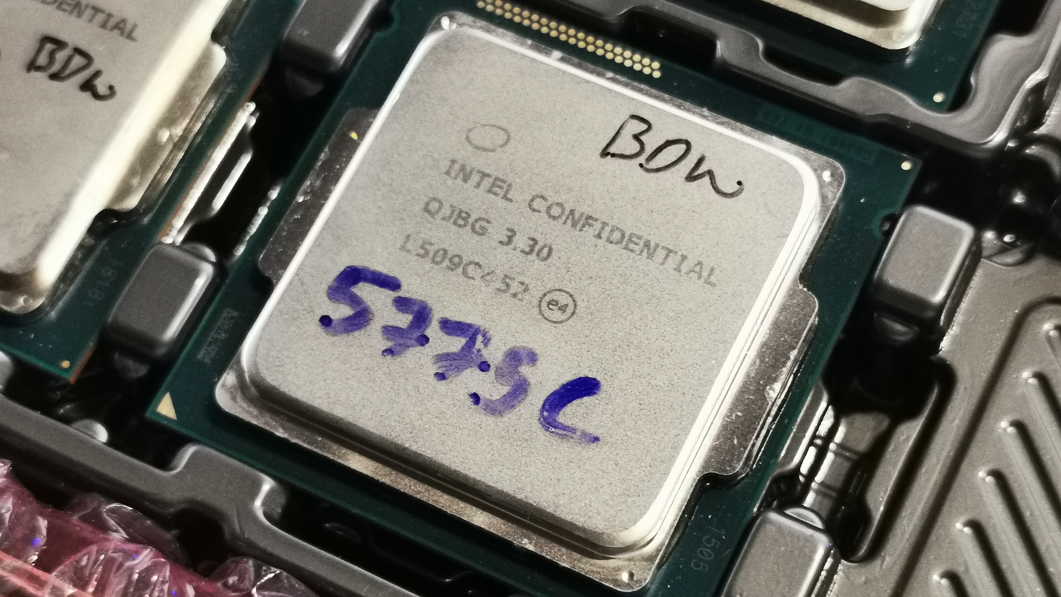
great reviewsadly i7-5775C's are still selling for $100+ on ebay. Not quite worth the upgrade over the i7-4790K, with graphics cards continuing to be by far the largest factor.
But to me it also shows there is no need to jump into the latest and greatest cpu, because these old cpus are still keeping up just fine.
plonk420 - Monday, November 2, 2020 - link
> sadly i7-5775C's are still selling for $100+ on ebayohhhh, that makes me curious as to how they compare to 3100/3300X chips now
Roy2002 - Monday, November 2, 2020 - link
So the conclusion is Optane could play a big role in future?Leeea - Monday, November 2, 2020 - link
no.Optane is slower then normal RAM.
Optane is a faster more limited version of an SSD. Specifically it has RAM like read performance in some areas, while having SSD like write performance in other areas.
Jorgp2 - Monday, November 2, 2020 - link
SSDs are much slower than Optane in writes.The worst case performance for Optane is better than the best performance for an SSD in writes.
FunBunny2 - Monday, November 2, 2020 - link
"The worst case performance for Optane is better than the best performance for an SSD in writes."may haps Optane will optimize when used with code compiled to use only memory-to-memory execution and no hard I/O?
Tomatotech - Monday, November 2, 2020 - link
I would have loved to see Intel embed a couple of gig of Optane on every mobo or in every CPU - at scale it would have been cheap - and we would get the benefits of instant app start, damn fast reboot etc. That would make a bigger difference to the end user experience than 15% on benchmarks. But no, it came out with poorly implemented tiering software, via expensive almost unused add-in cards. Optane had so much mass-market potential, sadly I think it’s screwed now for use outside the datacentre. Intel of all people should know how tiered storage works, why did they screw it up so badly? They even had a shining example in Apple’s Fusion drive to follow (copy) but still messed it up.Jorgp2 - Monday, November 2, 2020 - link
Have you considered asking supermicro for a skylake GT4e review sample?f00f - Monday, November 2, 2020 - link
That's intel's vision of "embedded" DRAM which is only a kind of embedded, because it is on a separate die. If you look for a proper implementation, look at POWER7 processor (2010) with L3 as eDRAM on the same die as cores.jospoortvliet - Wednesday, November 4, 2020 - link
I am a bit surprised amd didn't embed 32 or 64mb memory in the i/o chip... that would probably be relatively easy and affordable.