Imagination Announces B-Series GPU IP: Scaling up with Multi-GPU
by Andrei Frumusanu on October 13, 2020 4:00 AM EST- Posted in
- GPUs
- Imagination Technologies
- SoCs
- IP
It’s almost been a year since Imagination had announced its brand-new A-series GPU IP, a release which at the time the company called its most important in 15 years. The new architecture indeed marked some significant updates to the company’s GPU IP, promising major uplifts in performance and promises of great competitiveness. Since then, other than a slew of internal scandals, we’ve heard very little from the company – until today’s announcement of the new next-generation of IP: the B-Series.
The new Imagination B-Series is an evolution of last year’s A-Series GPU IP release, further iterating through microarchitectural improvements, but most importantly, scaling the architecture up to higher performance levels through a brand-new multi-GPU system, as well as the introduction of a new functional safety class of IP in the form of the BXS series.
The Market Demands Performance: Imagination Delivers it through Multi-GPU
It’s been no secret that the current GPU IP market has been extremely tough on IP providers such as Imagination. Being the only other established IP provider alongside Arm, the company had been seeing an ever-shrinking list of customers due to several factors – one being Arm’s extreme business competitiveness in offering both CPU and GPU IP to customers, and the fact that there’s simply less customers which require licensed GPU IP.
Amongst the current SoC vendors, Qualcomm and their in-house Adreno GPU IP is in a dominant market position, and in recent years had been putting extreme pressure on other vendors – many of these who fall back to Arm’s Mali GPU IP by default. MediaTek had historically been the one SoC vendor who had been using Imagination’s GPUs more often in their designs, however all of the recent Helio of Dimensity products again use Mali GPUs, with seemingly little hope for a SoC win using IMG’s GPU IP.
With Apple using their architectural license from Imagination to design custom GPUs, Samsung betting on AMD’s new aspirations as a GPU IP provider, and HiSilicon both designing their own in-house GPU as well as having an extremely uncertain future, there’s very little left in terms of mobile SoC vendors which might require licensed GPU IP.
What is left are markets outside of mobile, and it’s here that Imagination is trying to refocus: High-performance computing, as well as lucrative niche markets such as automotive which require functional safety features.

Scaling an IP up from mobile to what we would consider high-performance GPUs is a hard task, as this directly impacts many of the architectural balance choices that need to be made when designing a GPU IP that’s actually fit for low-power market such as mobile. Traditionally, this had been always a trade-off between absolute performance, performance scalability and power efficiency – with high performance GPUs simply being not that efficient, while low-power mobile GPUs were unable to scale up in performance.
Imagination’s new B-Series IP solves this conundrum by introducing a new take on an old way of scaling performance: multi-GPU.
Rather than growing and scaling a single GPU up in performance, you simply use multiple GPUs. Now, probably the first thing that will come to user’s minds are parallels to multi-GPU technologies from the desktop space such as SLI or Crossfire, technologies that in recent years have seen dwindling support due to their incompatibility with modern APIs and game engines.
Imagination’s approach to multi-GPU is completely different to past attempts, and the main difference lies in the way workloads are handled by the GPU. Imagination with the B-Series moves away from a “push” workload model – where the GPU driver pushes work to the GPU to render, to a “pull” model, where the GPU decides to pull workloads to process. This is a fundamental paradigm shift in how the GPU is fed work and allows for what Imagination calls a “decentralised design”.
Amongst a group of GPUs, one acts as a “primary” GPU with a controlling firmware processor that divides a workload, say a render frame, into different work tiles that can then the other “slave” GPUs can pull from in order to work on. A tile here is actually the proper sense of the word, as the GPU’s tile-based rendering aspect is central to the mechanism – this isn’t your classical alternate frame rendering (AFR) or split frame rendering (SFR) mechanism. Also, just how a single-GPU tile-based renderer can have varying tile sizes for a given frame, this can also happen in the B-Series’ multi-GPU workload distribution, with varying tile sizes of a single frame being distributed unevenly amongst the GPU group.
The most importantly, this new multi-GPU system that Imagination introduces is completely transparent to the higher-level APIs as well as software workloads, which means that a system running a multi-GPU configuration just sees one single large GPU from a software perspective. This is a big contrast to current discrete multi-GPU implementations, and why Imagination’s multi-GPU technology is a lot more interesting.

From an implementation standpoint, it allows Imagination and their customers a ton of new flexibility in terms of configuration options. From Imagination’s perspective, instead of having to design one large and fat GPU implementation, which might require more work due to timing closure and other microarchitectural scaling concerns, they can just design a more efficient GPU – and allow customers to simply put down multiple of these in an SoC. Imagination claims that this allows for higher-frequency GPUs, and the company projects implementations around 1.5GHz for high-end use-cases such as for cloud computing usages.
For customers, it’s also a great win in terms of flexibility: Instead of having to wait on Imagination to deliver a GPU implementation that matches their exact performance target, it would be possible for a customer to just take one “sweet-spot” building block implementation and scale the configuration themselves all on their own during the design of their SoC, allowing higher flexibility as well as a smaller turn-around time. Particularly if a customer would be designing multiple SoCs for multiple performance targets, they could achieve this easily with just one hardware design from Imagination.
We’ll get into the details of the scaling in the next page, but currently the B-Series multi-GPU support scales up to 4 GPUs. The other interesting aspect of laying down multiple GPUs on an SoC, in contrast to one larger GPU, is that they do not have to be adjacent or even near each other. As they’re independent design blocks, one could do weird stuff such as putting a GPU in each corner of an SoC design.
The only requirements for the SoC vendor are to have the GPUs connected to the SoC’s standard AXI interconnect to memory – something that’s a requirement anyhow. Vendor might have to scale this up for larger MC (Multi-Core) configurations, but they can make their own choices in terms of design requirements. The other requirement to make this multi-GPU setup work is just a minor connection between the GPUs themselves: this are just a few wires that act as interrupt lines between the cores so that they can synchronise themselves – there’s no actual data traffic happening between the GPUs.
Because of this, this is a design that’s particularly fit for today’s upcoming multi-chiplet silicon designs. Whereas current monolithic GPU designs have trouble being broken up into chiplets in the same way CPUs can be, Imagination’s decentralised multi-GPU approach would have no issues in being implemented across multiple chiplets, and still appear as a single GPU to software.
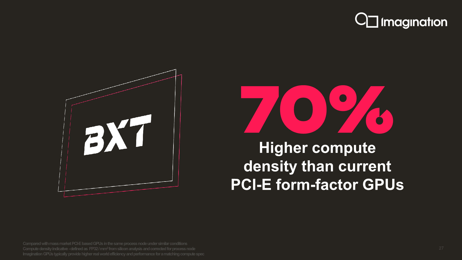
Getting back to the initial point, Imagination is using this new multi-GPU approach to target higher performance designs that previously weren’t available to the company. They note that their more efficient mobile-derived GPU IP through multi-GPU scaling can compete with other current offerings from Nvidia and AMD (Imagination promotes their biggest configuration as reaching up to 6TFLOPs) in PCIe form-factor designs, whilst delivering 70% better compute density – a metric the company defines as TFLOPs/mm². Whilst that metric is relatively meaningless in terms of performance due to the fact that the upper cap on performance is still very much limited by the architecture and the MC4 top scaling limit on the current multi-GPU implementation of the B-Series, it allows for licensees to make for smaller chips that in turn can be extremely cost-effective.
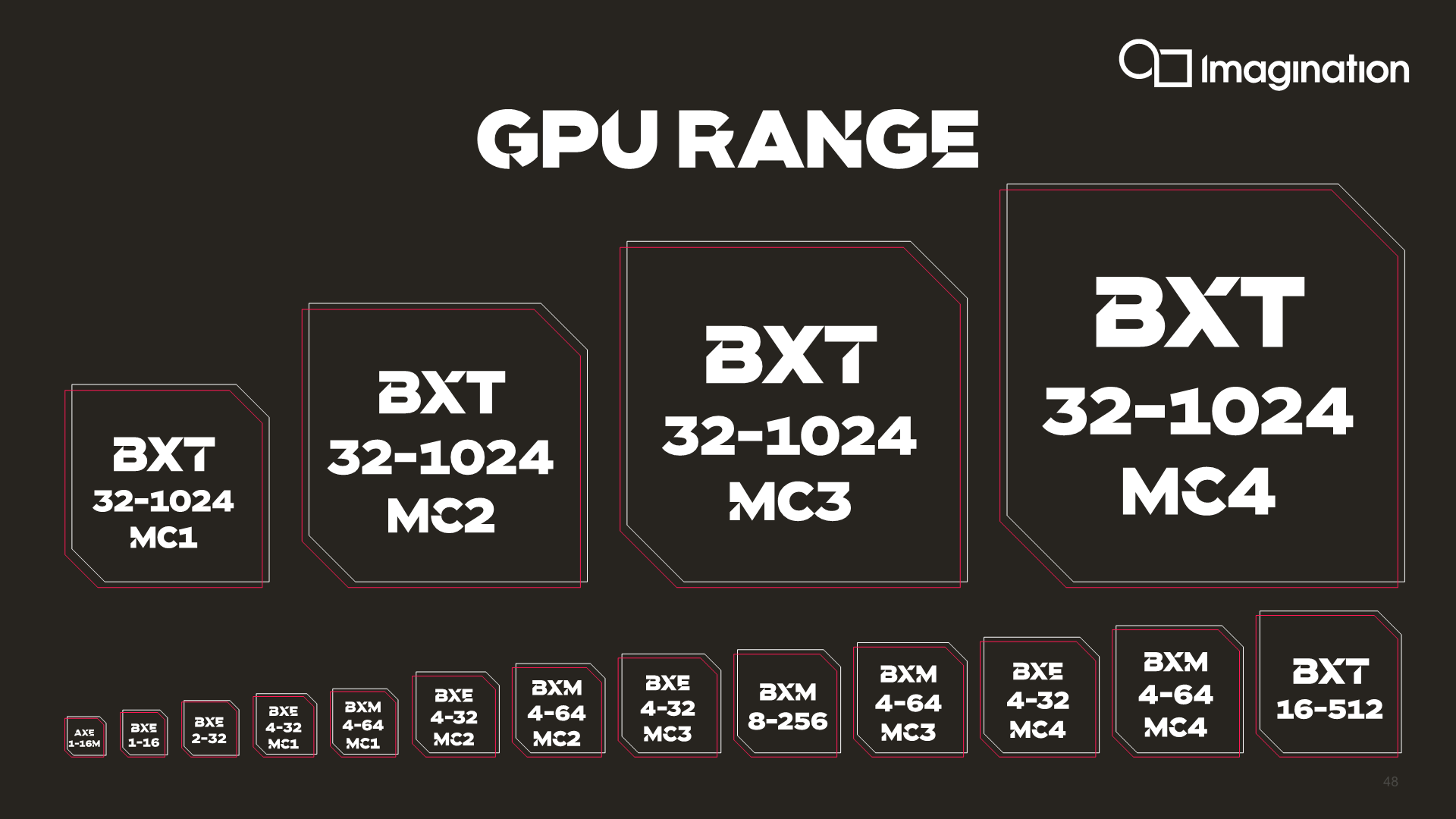
The B-Series covers a slew of actual GPU IP, with the company continuing a segmentation into different performance tiers – the BXT series being the flagship GPU designs, BXM series a more balanced middle-ground GPU IP, and the BXE series being the company’s smallest and most area efficient Vulkan compatible GPU IP. Let’s go over the various GPU implementations in more detail…


74 Comments
View All Comments
AMDSuperFan - Tuesday, October 13, 2020 - link
I would like to see some benchmarks of this product against Big Navi to help me make a good decision. So far, nothing seems to measure up.myownfriend - Tuesday, October 13, 2020 - link
The only places where it could really compare with Big Navi is if there's a game with a lot of overdraw that a maxed out B-series GPU would be able to rid itself of.persondb - Tuesday, October 13, 2020 - link
Honestly, I am not fully understanding as to how this GPU is supposed to compete in the high perfomance computing market. AFAIK, that market is hungry for tflops(as well as fast memory) yet this does not seem to deliver enough tflops.In fact, it's very disappointing specially for the tradeoffs that you would be forced to do in a multi-chiplet design. There are also a bunch of design decisions, that seem like they would hurt latency and possibly performance as well.
The article mentions that it has two possible configurations, one where a 'primary' GPU works as a 'firmware processor' to divide the workload across the other GPUs, in that kind of thing, it would seem to me that it would add some latency and overhead over the more traditional GPU. While the other configuration lacks a firmware processor but is completely limited by the primary GPU geometry unit.
Funnily enough, it don't seem like they have provided any detail about the memory controllers nor about the cache, possibly because it would be obvious that such a configuration would have it's severe tradeoff? There is also nothing about the interconnect that would link the GPUs together, this is an important one as it can have great impacts on the latency. You need to have them have some data sharing unless each GPU would only utilize the data it can get through it's own memory controller, but that could lead to problems too.
There are a bunch of things there that can increase latency and hamper performance. I personally would be skeptical about this until it releases and there are information on how this actually goes.
myownfriend - Wednesday, October 14, 2020 - link
This design is not forcing anybody to go with chiplets. These multiple GPUs can be placed on one chip. As far as peak TFLOPS and fast memory, my guess is that you aren't familiar with tile-based rendering, specifically Imagination's Tile-Based Deferred Renderer, does.AMD or Nvidia GPUs just pull vertices from external memory, then transform, rasterize, and fragment shade them then writing them back to external memory. All color and depth reads and writes happen in external memory. To make the most of that memory bandwidth and shader performance, game designers need to sort draw calls from near to far and maybe do a depth pre-pass to get rid of overdraw though there there will also be overdraw that occurs per draw call.
A tile based GPU pulls vertices from external memory then transforms them into screen space, clips and culls them, then write them back out into external memory as compressed bins that represent different tiles on the screen. It then reads them back a few tiles at a time and applies hidden surface removal on opaque geometry to remove overdraw completely. That process creates an on-chip depth/stencil buffer which insures that only pixels that contribute the final image get submitted for fragment shading. It then attempts to create the back-buffer for that tile completely within a small amount of on-chip color buffer memory so that it only needs to write back the finalized tile to external memory.
The depth buffer never even has to get written to external memory, all overdraw for opaque geometry is completely removed regardless of the order they were submitted to the GPU, and the 6TFLOPs that the B series can theoretically achieve is being spread among fewer pixels. It has far less reliance on external memory bandwidth since it only really needs to use it read textures and geometry data and store the tile list. Since on-chip memory can potentially use very high bus widths and run in-sync with the GPU, they could easily provide more bandwidth than GDDR6X memory. At 1500Mhz with four GPUS and four tiles per GPU, a 256-bit bus to each tile would feed it with 768GB/s of low-latency memory bandwidth. If you're curious how large each tile is, previous Imagination GPUs used 32x32 pixel tiles or smaller so a 256-bit G-buffer would only require about 32KB per tile so it can just use SRAM.
That tiling process also provides a simple way of dividing up the work among the GPUs. You mentioned that configuration that uses a primary GPU. The article says that would be the only one with a firmware processor and a geometry front end so it would be the one that handles all vertex processing and tiling but after those tiles are written to main-memory, the only communication that it needs to make with other GPUs is to tell them to read some of those tiles. They can then work almost completely independently from each other.
To my knowledge, even per compute workloads can take advantage of those on-chip buffers as a kind of scratchpad RAM.
Threska - Wednesday, October 14, 2020 - link
I remember this discussion with my Apocalypse and PowerVR. Shame the idea never really took hold.persondb - Friday, October 16, 2020 - link
Modern GPUs since Vega and Maxwell already use a hybrid of tile based rendering and more traditional rendering methods(you can see this old-ish video on nvidia approach https://www.youtube.com/watch?v=Nc6R1hwXhL8). IDK why you commented on it. Since that means it's not a straight comparison of Tiled vs traditional methods.I mentioned TFLOPs for compute workloads and not those graphical workloads, which was described in the article as being one of the potential markets for this. As far as I am aware, a gpu that is tile based wouldn't change much for pure compute workloads.
Also about that memory, I really doubt with that kind of configuration the latency would be that low. Probably higher than you expect. Though of course, GPUs generally aren't latency sensitive as CPUs. But it's also not that much higher than something with GDDR6X(or just GDDR6 with some 16 gbps chips).
I must say that I am not familiar with tile based GPUs, but say per example about textures. Obviously you need to get them from the external memory, as there is no SRAM in the world that could store all textures that you need. This would obviously complicate the memory controller issue as I was talking about in my original post. Same for say computing with large memory requirement.
Obviously, if each of the chiplet has their own (say 64-bit) memory controller then they will need an interconnect to share the data. And that is what I was talking about, such a thing would increase latency. And again, the article does not say how the memory controllers are set up for those chiplets.
myownfriend - Friday, October 16, 2020 - link
Tiled caching and tile-based rendering are still very different. Tiled caching can't do that and I believe it only works on a small buffer of geometry at a time as it works completely within the 2MB of L2 cache which is not enough to store the geometry for a whole scene. It's enough to have reduced the required external memory bandwidth by quite a bit. Tile-based rendering creates the primitive/parameter buffer in external memory before pulling them back on chip tile by tile and has the ability to create the entire back-buffer for each tile completely within on-chip memory.https://www.imgtec.com/blog/a-look-at-the-powervr-...
In modern games, textures and geometry take up a lot of space in RAM but account for very little of the used memory bandwidth. Textures are generally compressed to 4 bits per pixel (though ASTC allows bit rates from 8 to 0.89 bits per pixel) and are read once to a few times at the beginning of the frame. The majority of bandwidth is needed for the back buffer which, for an Ultra HD game with a 256-bit G-buffer, would only take up about 265 MBs of space but would be written to and read from multiple times per-pixel per-frame. That's why the Xbox One had 32MB of ESRAM with a max bandwidth of 205-218GB/s and 8GB of DDR3 over a 256-bit bus with only 68.3GB/s of bandwidth. The ESRAM was large enough to store a 128-bit 1080p g-buffer and the DDR3 stores textures and geometry and acts as work RAM for the CPU. If a game has low-quality textures these days, it's generally blamed on the amount of RAM not its speed. As resolution increases, the average texture samples per-pixel goes down. In other words, if the chiplets do need to fetch texture samples from each other then it wouldn't require all that much chiplet to chiplet bandwidth. Using that XBO as an example, that's 17.075 GB/s per 64-bit memory controller without accounting for the fact that the CPU is using some of that. That's 40% of the die to die bandwidth between AMD's Zeppelin chiplets. TBDR would decrease texture bandwidth even more because it only fetches texels for visible fragments.
I'm not sure what you mean by "Also about that memory, I really doubt with that kind of configuration the latency would be that low. Probably higher than you expect." Are you talking about how said that the on-chip memory is ultra low-latency and high bandwidth? Because it would absolutely be low-latency. We're talking about a very local pool of SRAM that's running at the same clock as the ALUs. Meanwhile GDDR6X would have to be accessed via requests from memory controllers that are being shared by the whole chip then traveling off-package, through the motherboard and then into a separate package and back.
You're right about compute workloads not being all that different between TBRs and IMRs so a compute load that generally needs a lot of high bandwidth memory would still have the same requirements for external memory. However, I'm lead to believe that the reason GPUs are used for compute workloads is because those compute workloads, like graphics workloads, are considered embarrassingly parallel so I don't really know how much data moves horizontally in the GPU. It is very possible that most GPU compute workloads could be modified to make some use of the on-chip storage to reduce reliance on external memory.
I'm also curious to see how those memory controllers are set up, too, but I'm a bit more confident in a TBRs ability to scale in a multi-GPU set up.
myownfriend - Wednesday, October 14, 2020 - link
The last time Imagination's GPUs were in the desktop space was in 2001 with the Kyro II. GPUs then and now are very different but this article can still give you a sense of what sort of gains a TBDR GPU could potentially provide.https://www.anandtech.com/show/735/10
Compared to the Geforce2 Ultra, the Kyro II used under half the amount of transistors, under half the power, had 36% of the memory bandwidth, 35% of the fill rate, and cost 44% of the price yet it actually beat the Geforce2 Ultra in some tests especially at higher resolutions.
eastcoast_pete - Wednesday, October 14, 2020 - link
One area currently grossly underserved by both NVIDIA and AMD is in entry-level dGPUs with decent ASICs for HEVC/h265, VP9 and AV1 decode in 10bit HDR/HDR+ on board. Basically, PCIe cards with 2-4 Gb VRAM under $ 100 that still beat the iGPUs in Renoirs and Tiger Lakes (Xe). That market is up for grabs now, maybe these GPUs can fill that void?vladx - Wednesday, October 14, 2020 - link
Video encode/decode is one of the features used by cloud GPUs so it would most likely be able to do all that.